Lab 3
Quick Stats
Time Spent: 21 Hours, 45 Minutes, 57 Seconds
SystemVerilog Modules: 10
Total FSM States Created: 16
Testbenches: 5
Time Wasted on a Busted Keyboard: 1 hour 13 minutes
Mind Melting Bugs: 2
Buttons Mashed for Testing Purposes: a lot
Overall: Success
See my Blog Reflection for more!
Lab 3: Keypad Scanner
Lab Task: Out with the Switches, In with the Keypad
Recall that in Lab 1, students used their FPGA to control a seven segment display. Lab 2 added an additional layer of complexity, asking students to double the inputs and double the displays without doubling the hardware and GPIO burden.
Lab 3 gives students a straightforward task. Maintaining the dual display system, swap out the 8 switch inputs for an 8-pin, 16 button keypad. With the goal in mind, let’s dive right in!
Understanding the Hardware
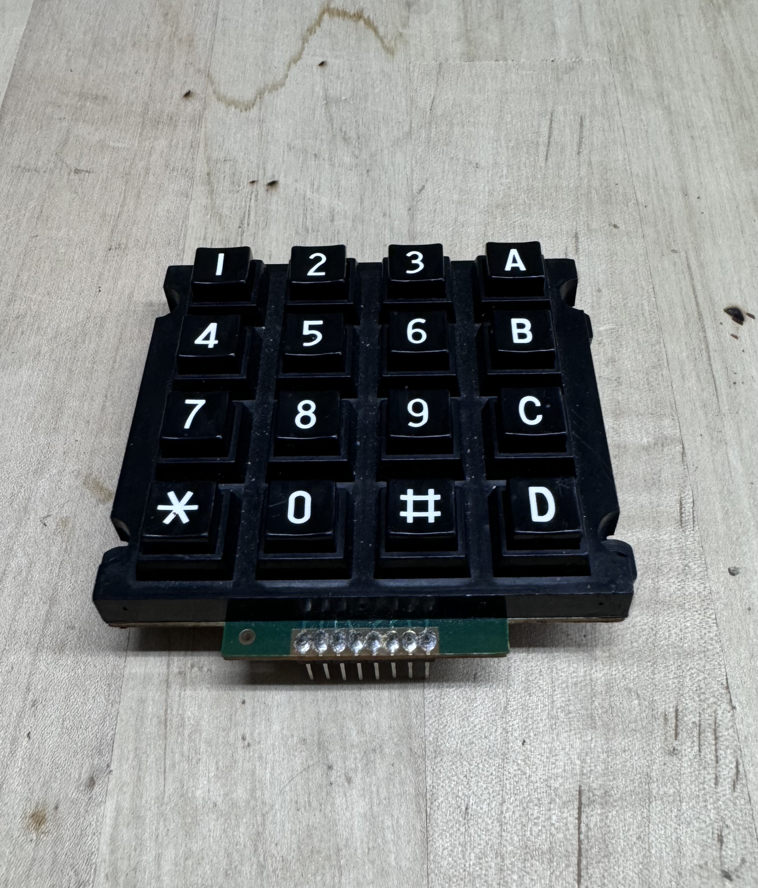
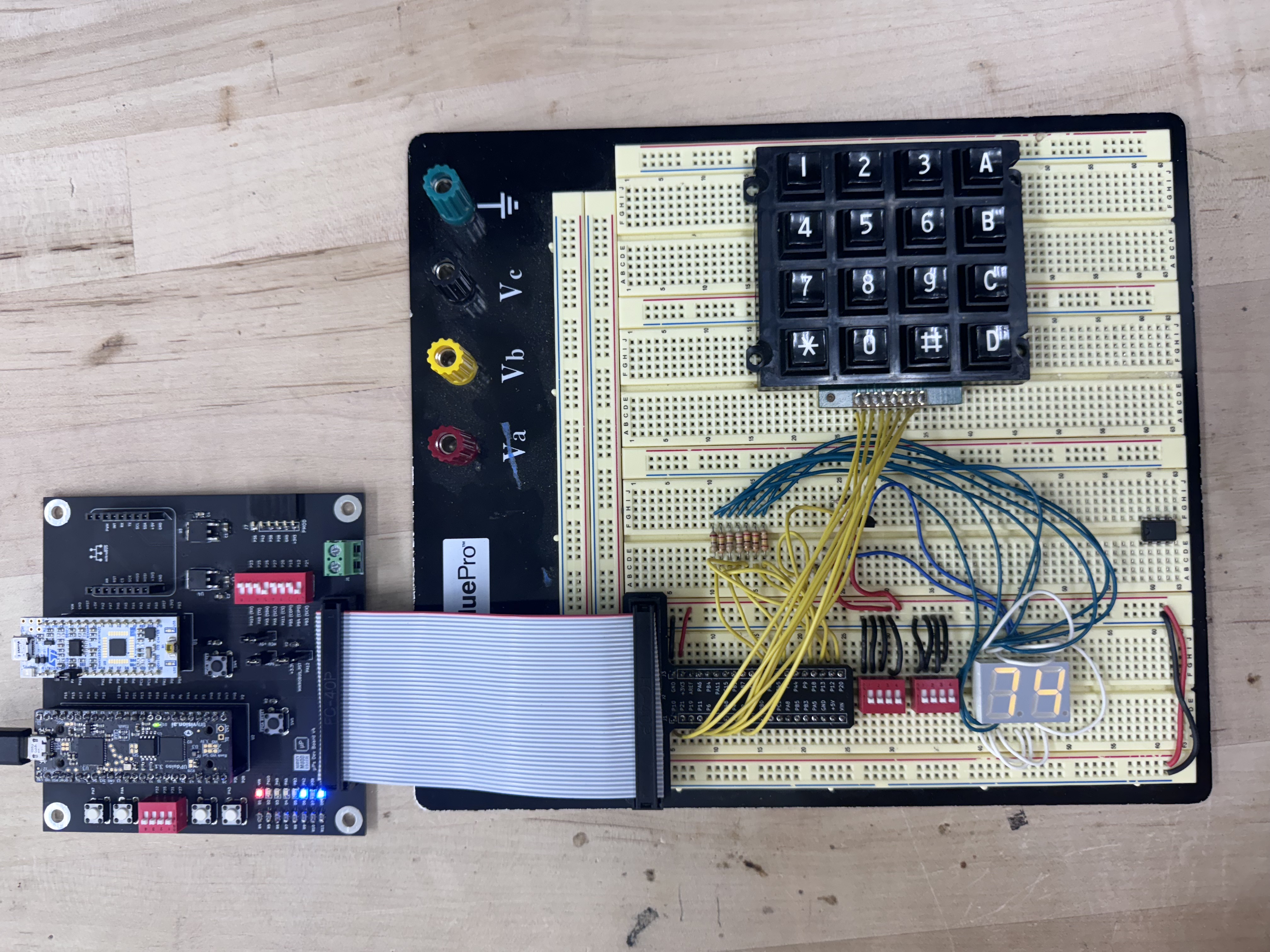
The keypad took me some tinkering to understand fully. Pictured above, it has 8 pin outputs, labeled 1 to 8 from left to right. The pins create a 4x4 matrix, where each node represents a switch. Pressing a particular button connects that node’s column line to that node’s row line. In this way, each of the 16 buttons may be represented by a unique connection between one row line and one column line. By using a multimeter to reveal continuity, I created the following scratch note sheet for myself, describing the connections that each button makes between each pin. Note that the layout in Figure 2 below matches the orientation of the buttons in Figure 1 above.
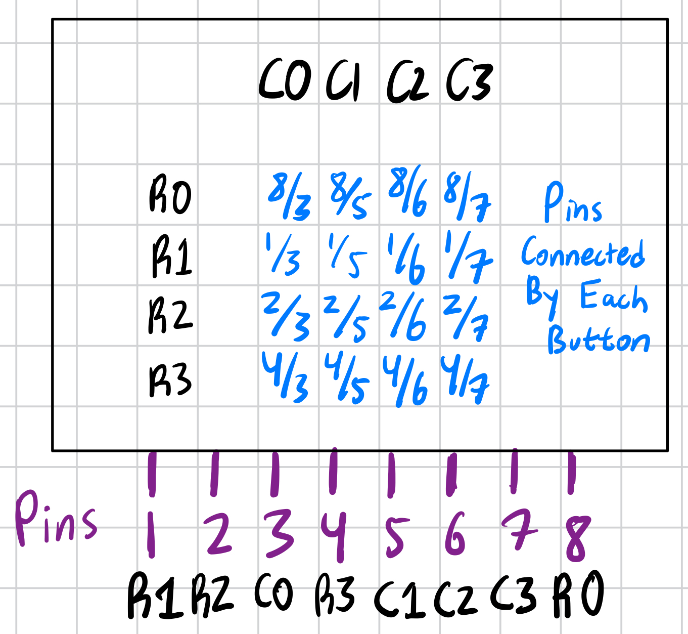
So, the question then becomes – how does one detect these pin connections as they happen? Consider if you set all of the column pins to a logical high, and left the row pins logical low. Pressing one button, say the number 1, would connect the Row 0 and Column 0 lines together. Thus, the logical high value could pass from the column pin 3 to the row pin 8, where it could be read out as an input. However, how would you know which button in the row was pressed? You would have no way to determine whether the connection was made by the 1, 2, 3, or A button, any of which would connect a logical high column to Row 0. Instead, one could imagine setting all of the row and column pins to low. By setting only one column pin high at a time, you allow the input row pins to determine which button is being pressed. If Row 1 reads in a logical high while only Column 2 is similarly high? The user must be pressing a 6. If the user holds down this 6, the row pin should only register an input every time the high column pin cycles back around. By scanning through each column in sequence, we can thus read out all 16 buttons on the keypad. Figure 3 below shows some of this in more detail, diagram-style.
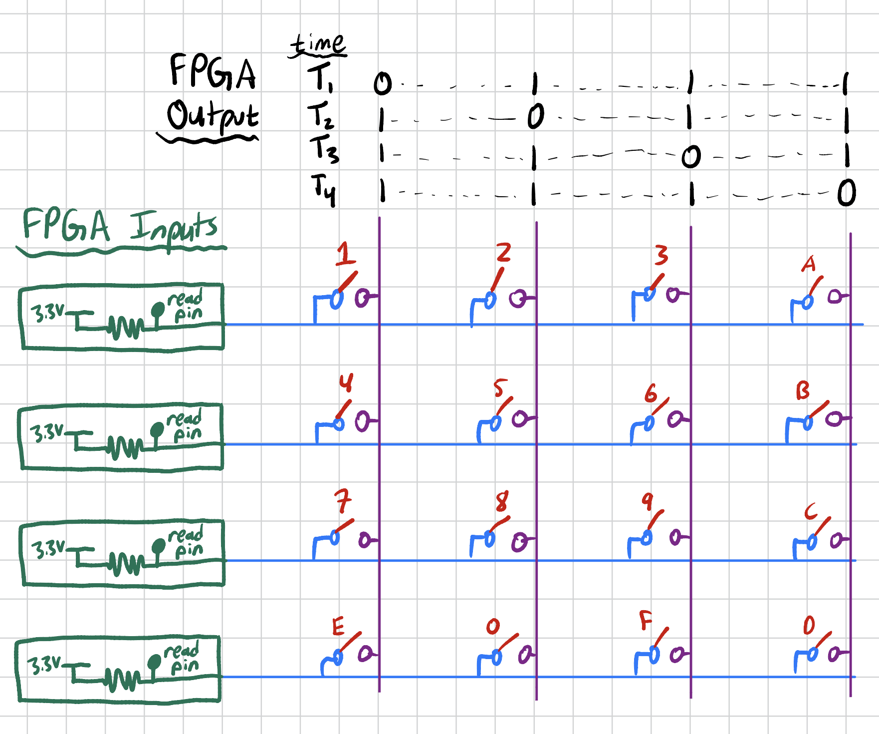
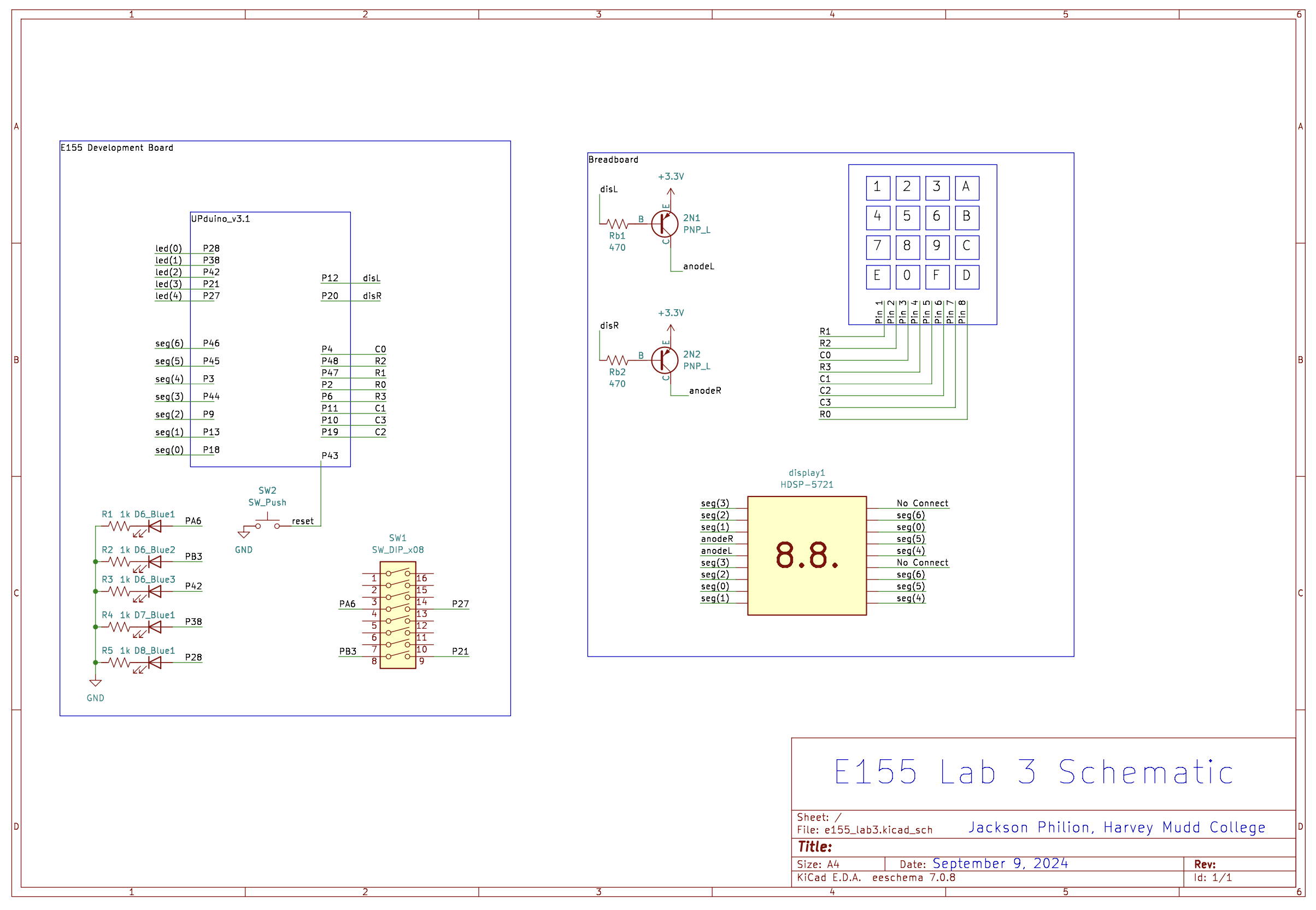
One might note that Figure 3 seems to show the columns scanning through a single logical low bit, rather than a logical high. Knowing that the FPGA pins have internal pullup resistors, I opted to switch the polarity of the logic. I opted to keep all of the keypad columns logical high, and scan through with a single logical low value. I could then read any logical low row pins as an input button pressed. I made sure I had a reset set up, reused the same display multiplexing schematic from Lab 2, and wired up my keypad to the same pins the switches used to occupy. I kept the LEDs in use on the E155 protoboard, using them as a debugging tool. Figure 4 below shows the schematic, which may be viewed in more detail under the notes and extras folder in my Github.
Dealing with Bounce
One key flaw in most any physical button or switch hardware is its tendency to bounce. Bounce is when a connection is made and broken multiple times over a very short timespan, often occurring when a connection is first made or first released. Taking our buttons, for example, they have a springing mechanism which keeps them open. When they are depressed, they make a satisfying click. This is the physical deformation of the button, going from one relaxed “on” state to a similarly relaxed “off” state. The stage in the middle is unstable, and forces act to drive it either fully open or fully closed. These forces, coupled with the spring mechanism and rigid nature of the button, cause this bounce phenomenon as a button snaps and unevenly settles between states.
Software designers need to have an understanding of debounce techniques in order to code robust software which is capable of ignoring bounce. For example, you wouldn’t want 10 “b” letters logged in the span of a microsecond. It is safe to assume that those repeated loggings were due to bounce, and should represent only one button press. On the other hand, maybe two or three button presses in a second are possible, and must register as distinct inputs. To find the difference between a bouncing input and a steady, true input, I decided to use a counter system. When enabled, this counter system initially gains some middle value. As the clock cycles, every time the input matches a true button press, the counter ticks up. If the button indicates a false input, or a still bouncing button, the counter ticks down. The counter module reads out a result if its value reaches either the upper bounded top rail, or the lower bounded bottom rail, indicating either a true input or a false input respectively. Figure 8 in the System Design section below shows the diagram of this system.
This would not be the only way to account for debouncing. One other way to avoid logging false inputs would be to slow the whole system down, making each clock cycle significantly longer than the time a button would take to bounce. However, I did not like this option. First off, the counter system gives me an easy knob to tune – the value at which the counter starts, and the value of the top rail. By adjusting these values, I can test my hardware to find the right balance between delay and speed without affecting the rest of my system. If I were to implement a slow clock system to account for bounce, my adjustment parameter then affects the entire system. This is undesireable. Additionally, I was worried about imperfect and rocking buttons momentarily disconnecting the input button as it was held down, causing an additional form of bounce and reconnection that would register as an additional press. I feared that this slow clock system would be more liable to register such an intermediate bounce as a new button click, since it had less data to use as a reference.
Another way to address bounce would be to wait a fixed time before reading in the input again. This gives the designer control over a similarly easy-to-tune parameter, and mimics the method often used in many DIP push button MCU systems. In my case, however, I again felt that collecting and comparing more data was better than comparing less data. By sampling the signal multiple times with my counter, I make sure that I am not beholden to any single cycle of bouncing.
System Design
In this lab, the challenge is implementing this system into hardware. In order to describe how information is stored and passed, I created a Moore Finite State Machine (FSM). The FSM diagram in Figure 5 below illustrates my scanning system, polling through each column of the keypad. Note the general stage titles of the system on the left. This scanning through the columns is the core of the system, in scanColsX. The addition of synchronizers on the input necessitate the addition of two boot states to delay the system. If a valid input is read in, the system kicks over into the verification stage, where the goal is to make sure that the signal is one valid button pressed. This stage attempts to account for button debounce, which is discussed later in this lab. If the input is valid, the system then moves into the Set and Hold stage, where the input is sent out to the seven segment display and the system is placed into a holding state until all buttons are unpressed.
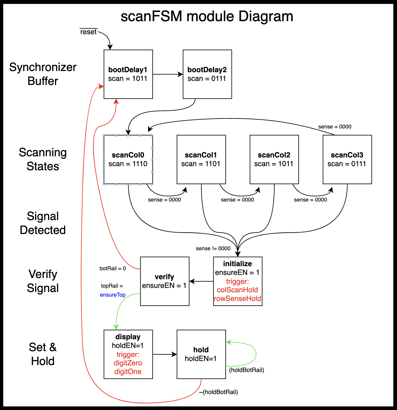
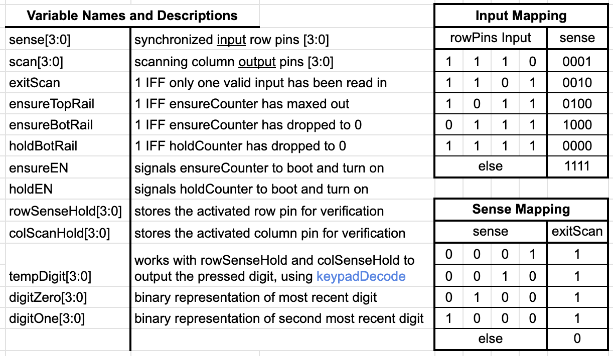
Translating this into clear and specific inputs and outputs, the state transition table in Figure 7 below describes the specifics of the system. Figure 6 describes the inputs with some simple matrices and describes each of the variables in the table.
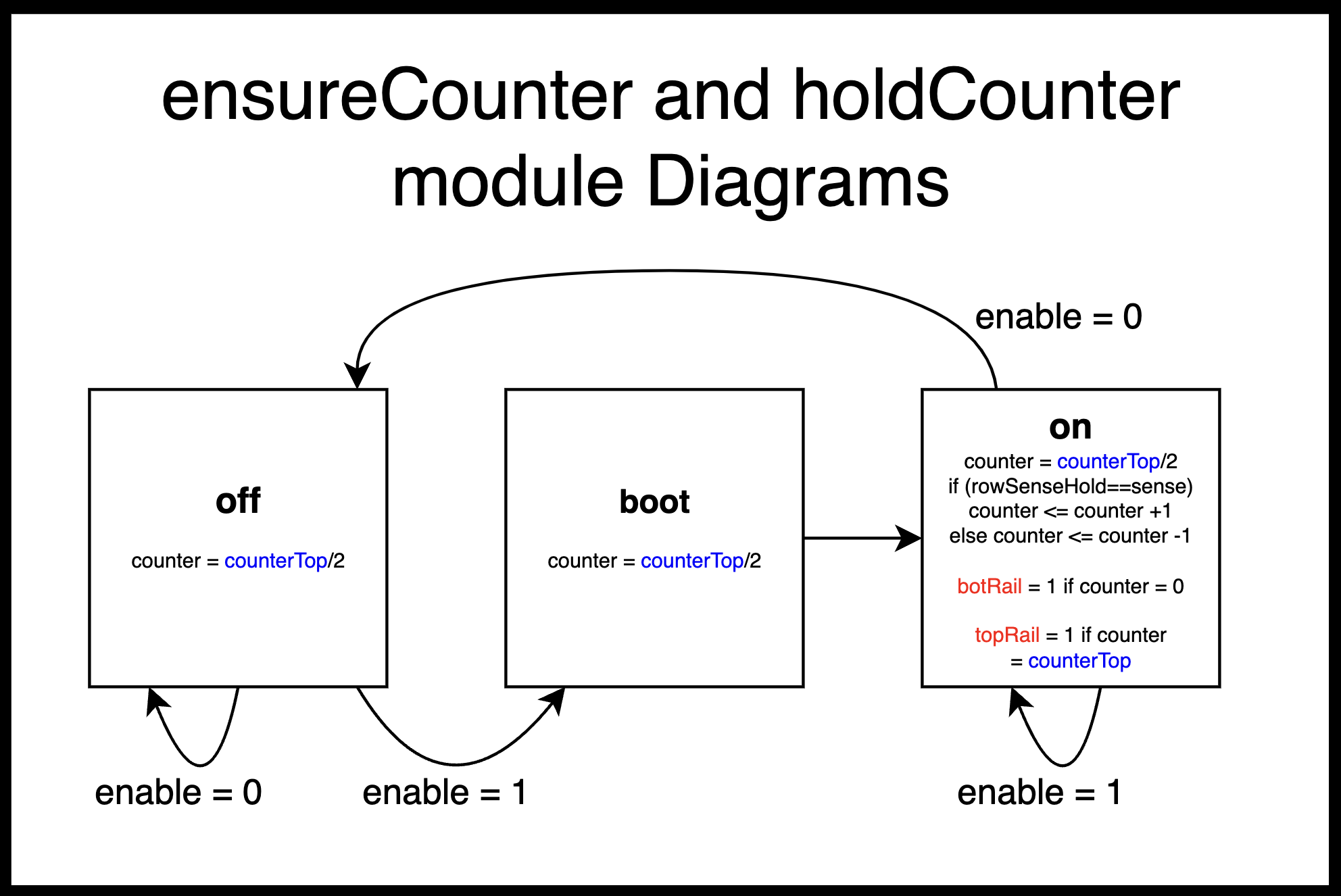
Additionally, I wanted to flesh out the counter modules, since they would need simple FSMs of their own. Since they are relatively similar, Figure 8 describes both modules by the same general diagram.
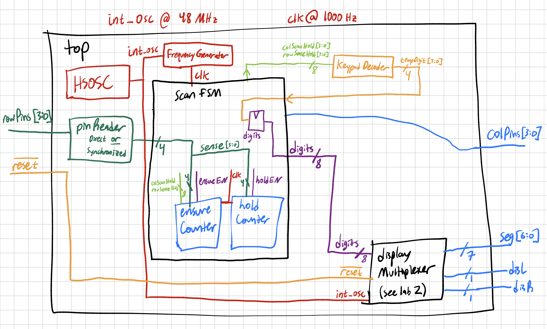
Finally, I needed to sketch out how each module connects using a block diagram. Note that this block diagram isn’t nearly as neat as I would normally prefer – however, in this lab, the real meat and potatoes is in the FSM diagrams. The block diagram in Figure 9 below merely serves to show how the wires connect in SystemVerilog. Note that int_osc and clk signals are different, accounting for the fact that the display multiplexer runs at a different frequency than the keypad scanner. Funnily enough, in the end, I ended up using the same value of 1000Hz for both. Therefore, I could have cut down the extra frequency generator inside the display module.
Having designed the system, it was time to put it into SystemVerilog! The full contents may be found in the FPGA folder of my lab 3 Github repository, found here. Note that there are two main branches, corresponding to my code before synchronizers and after synchronizers.
Simulation
Simulating this lab was a doozy, but essential to the lab’s success. Without simulation, it would have been near impossible to tell what was happening in my hardware. An oscilloscope helped me see the scanning of the columns, which coupled nicely with my onboard indicator LEDs and a reduced 1Hz clk signal to give me a debugging suite. My simulations all went off nearly without a hitch – I mainly spent my time fixing small syntax errors. The design work beforehand paid off!
Starting with the simplest module, I tested the keypad decoder module in Figure 10 to verify that for a given column and row input, it outputs the correct hex input digit.
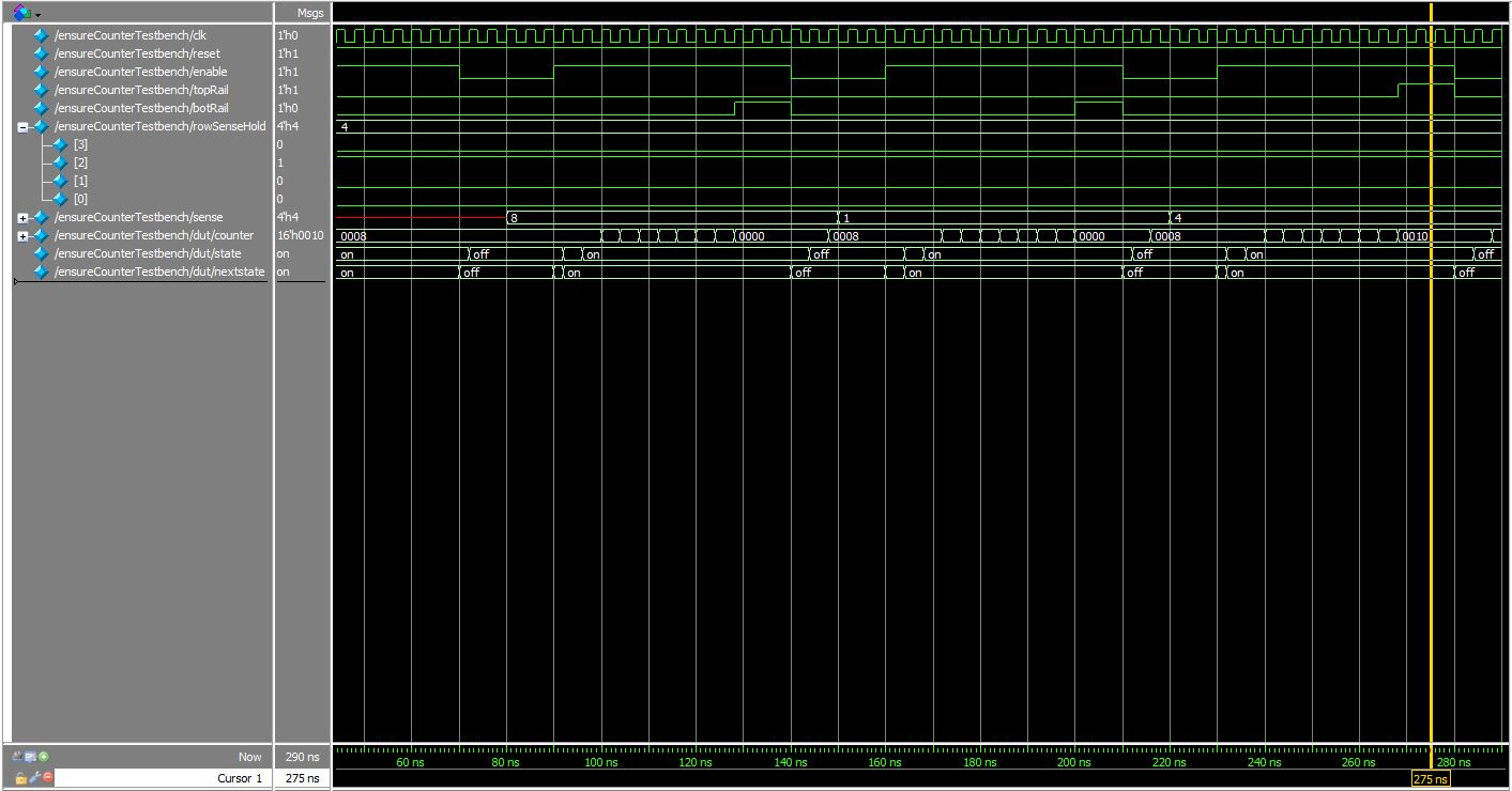
Moving onto the ensureCounter module, I verified that it cycled through states properly, activated its top and bottom rails as necessary, and counted as desired. It performed smoothly!
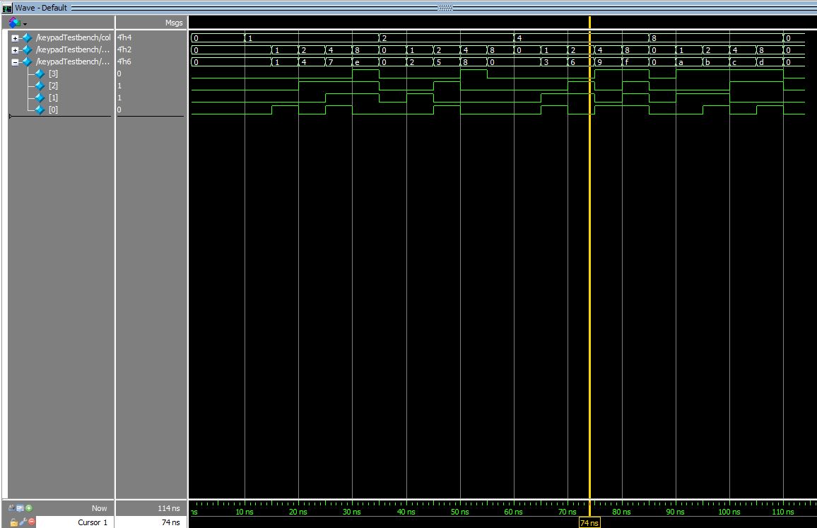
Moving now to the bigger beast, scanFSM, I loaded it up and was surprised to see that it too simulated after only a few small syntax or inversion errors. Note that this does not yet include the synchronizers. Specifically, referring to Figure 12, I checked to make sure the states cycled as expected, the correct row and column were held at the proper time, the intended digit was read out into the display input, and that it integrated with the counters to verify any button presses.
Putting this into hardware, it worked! I had some issues at first with a prolonged button press with several intermediate presses registering as multiple presses of the first button. Changing my default case in the pinReader module fixed this issue. Additionally, I had some issues with my state register when I synthesized it with Lattice Radiant and uploaded it to my FPGA. Strangely, the software did not warn me and I was stuck for quite some time. After more clearly defining all of my defaults, the system worked. I predict that the synthesizer was recognizing my creation of an FSM and attempting to optimize the state encoding and logic – unfortunately, this caused some of my default cases not to apply as they should have. After speaking with Professor Brake, he hinted that this may just be an unfortunate quirk of the software.
Synchronizing the Inputs
Finally, the trickiest excellence specification for the week asked students to add in synchronizers to their inputs. A synchronizer is a mechanism to avoid metastability in a synchronous system with asynchronous inputs. In our case, all of our keypad presses were asynchronous inputs, and reading them on a clock edge as they changed could put our synchronous logic into a dangerous middling state, where the logic recognizes it as neither high nor low. This can propagate and ruin systems, or at the very least, cause some incorrect bits when it does occur. However, most metastable inputs settle over time. The goal of a synchronizer is to increase this settling time on the input before introducing it into your system. By stringing the input signal along between, say, two flip flops, you can give the input signal two additional clock cycles of time to settle to a logical low or logical high. So, that’s exactly what I did!
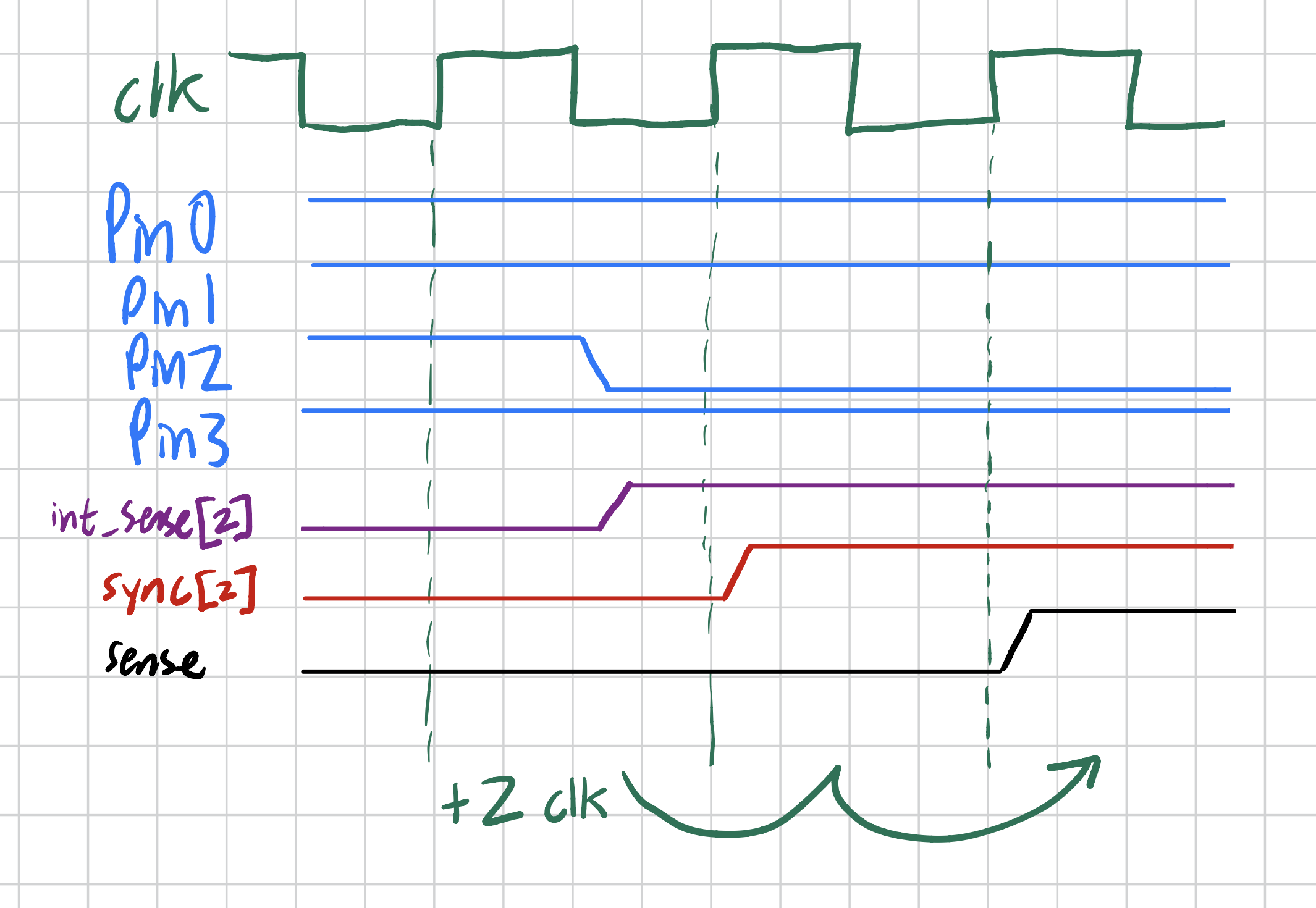
However, introducing synchronizers adds an additional layer of complexity to the system. As Figure 13 illustrates, these synchronizers delay the inputs into my system. As I scan along the columns, there is now an introduced two cycle delay between when my input reads out and when my FSM registers it. Referring to Figure 5, one can see that an input read into scanCol1 would not register until the system had moved onto scanCol3. That is to say, the delay mismatches the “scan” value at any given time with the “scan” value which correlates to the currently read input. In order to solve this, I added in two registers which store the two most recent prior values of scan. Thus, by referencing back to the value twoPriorScan, I can properly match the delayed input sense with the delayed output scan.
However, this in and of itself is not enough. The FSM in Figure 5 thus needs two cycles to load in the most recent input and output values. So, I gave the system two extra cycles to boot and store new information before it drops into its regular scanning cycle. Likely, I did not need these additional stages. I may have gotten away just fine by letting it loop back, and building in more conditions into how the system moved into the initialize stage. However, I found it simpler and easier to understand if I instead added two boot delay states.
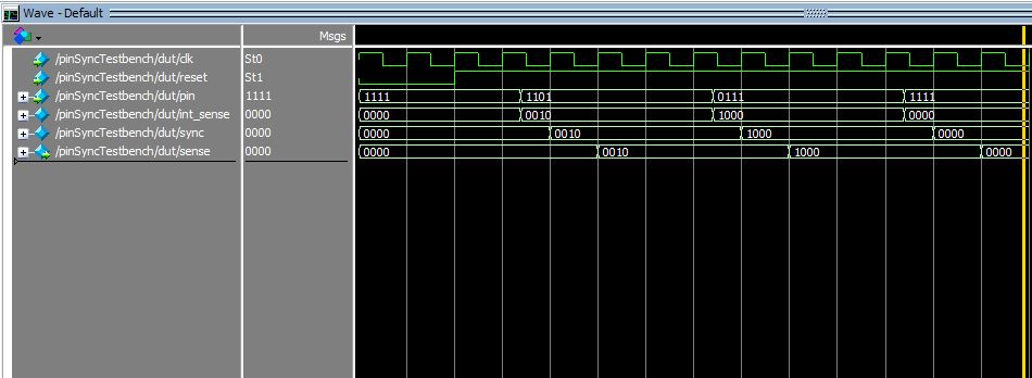
As I coded these synchronizers into SystemVerilog, I again wrote some simple testbenches. The first one, in Figure 14 below, shows the intended two cycle delay and polarity flipping on the new pinReader module.
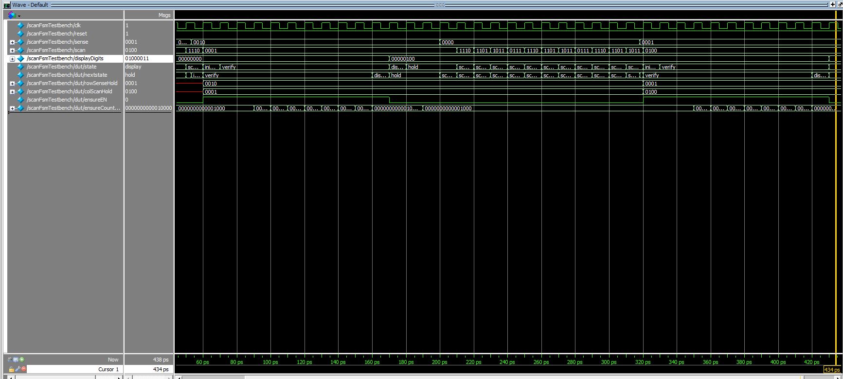
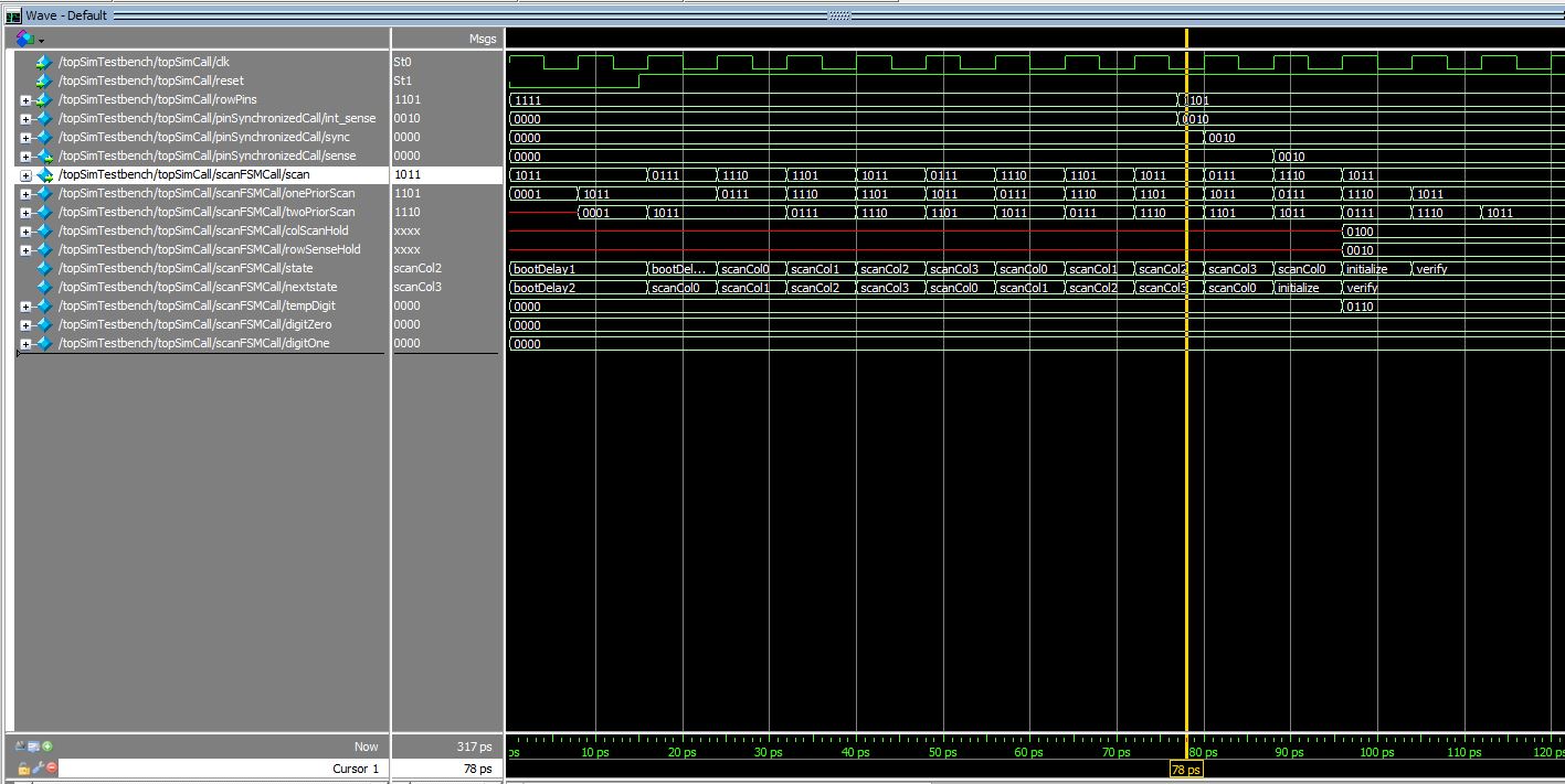
Finally, Figure 15 shows a successful run of the top module with all synchronizer code built in.
Final System and Conclusion
And with that, I had my final system! My blog post for Lab 3 contains more details about the second mysterious bug that I encountered, and my feelings on the matter. This lab wasn’t as frustrating as I think it was for some – although I encountered my share of confusion, I always felt like I had a clear path forward. My final system is incredibly robust, successfully able to avoid many forms of multiple-button presses while responding to valid inputs in a snap. I wish that I could have been better able to deal with two simultaneous button presses in adjacent columns. In fact, I am surprised that the system seems to handle it as well as it does. I’m not exactly sure what causes it to ignore simultaneous adjacent column presses. However, I did successfully add synchronizers, avoid logging interstitial short presses over longer simultaneous presses, and ignore simultaneous presses along different rows. I’m proud of my work in this lab, although I recognize that there is room for improvement, both in terms of functionality and FPGA efficiency.