Quick Stats
Time Spent: 18 Hours
SystemVerilog Modules Written: 4
Software Installs/Tutorials: 4
Testbench: Eventual Success
Overall: Success
See my Blog Reflection for more!
Lab 1: FPGA and MCU Setup and Testing
*Note: You can find all the source code from Lab 1 in my Github here.
Prelab Skills
Lab 1 introduces students to some foundational elements of the class before asking them to do their first piece of generative design work. Chiefly, it introduces students to three key softwares that will be essential to success throughout the rest of the class:
The FPGA design software Radiant Lattice, which is used for implementing designs onto the FPGA and mapping pin ins and outs. This is new to most students.
The MCU design system SEGGER Embedded Studio, which most students have experience with but have not yet connected to an ARM processor.
Git and Github tools, which is a required organizational tool in this class due to its importance throughout personal and professional work in coding and electrical engineering.
Quarto website builder, a software system added as an extension to VSCode which has allowed me to build up this portfolio.
For all intents and purposes, I was a complete beginner with all three of these tools. Thus, the majority of my work in Lab 1 was spent combing through posted class tutorials, checking with online walkthroughs, and building shorthand cheat sheets to help contain the rush of new information. The good news? I now feel comfortable building a raw .sv file from scratch and using Radiant Lattice and Modelsim to integrate and push it to the FPGA. I also feel more confident than I should about building out a test bench – I have yet to integrate an automated one successfully, but I can imagine what I will change for my next iteration in lab 2. It successfully compiled but failed to pull in my testvector.tv file. I realize now that it was in fact a hidden testvector.tv.txt file – Windows has to stop hiding extensions! I also have numerous working testbenches to pull from in my E85 digital electronics work, and thoroughly enjoyed the satisfaction back then of writing a thorough test bench! All that is to say, I am excited to refine my testbench next week and feel confident that I have a route forward. This lab did not involve SEGGER to any significant degree, so I will hold off discussion of that software until a future week.
I have also built a basic level of fluency with git – I’m happy to report that the cheatsheats barely get any use! Initializing, adding, branching, committing, pushing and pulling are second nature at this point. This was due partially to a hugh warm up period in which I accidentally created 4 different repositories for Lab 1. Combing through this mess to understand what happened and how to fix it contributed significantly to my learning. I still have to look up some commands for finding the correct remote address, and sometimes find myself using the GitHub desktop app for some arranging. However, I mostly use the bash command terminal, and have gotten comfortable interfacing with the lab computers to continue coding projects across any desktop I choose. I still need to build significant fluency with merging and managing branches after creation. I can walk through the steps, but I am left uncomfortable with more than one branch left open at a time and often delete branches immediately after their creation. I think I have yet to fully understand how branches will be a benefit to my work.
Quarto is also a work in progress. Consider the design of this page my first real world test of this skill – did I succeed? How can I improve? This is what I will ask myself in preparation for my lab 2 page next week.
Lab Task: Seven Segment Display
After the preliminary skills introduction, the primary task of Lab 1 is rather simple.
The task:
- Take as an input 4 switches, set in order to each represent a consequitve input bit.
- Control a seven segment display to read out the 16 hexidecimal digits from 0 to 15 (or h0 to hF), which correspond to the 4 bit input.
- In addition, control 3 onboard LEDs to obey the following truth tables with relation to the switch inputs:
| S1 | S0 | led[0] |
|---|---|---|
| 0 | 0 | OFF |
| 0 | 1 | ON |
| 1 | 0 | ON |
| 1 | 1 | OFF |
| S3 | S2 | led[1] |
|---|---|---|
| 0 | 0 | OFF |
| 0 | 1 | OFF |
| 1 | 0 | OFF |
| 1 | 1 | ON |
| led[2] |
|---|
| Blink at 2.4 Hz |
With the task laid out, and my skills adequately built up, I tackled the lab by first attempting to understand the seven segment display.
Understanding the Display, Inputs, and Outputs
I began my task by trying to understand the seven segment display. This would give me an idea of how many signals I needed to run to it, and how to map out a truth table which would describe each hex number. My selected display unit had a clearly printed serial number on it, which corresponded to the following Jameco Link and the following data sheet. Based on these resources, I derived that I could control the segments of my display via the following pin mapping:
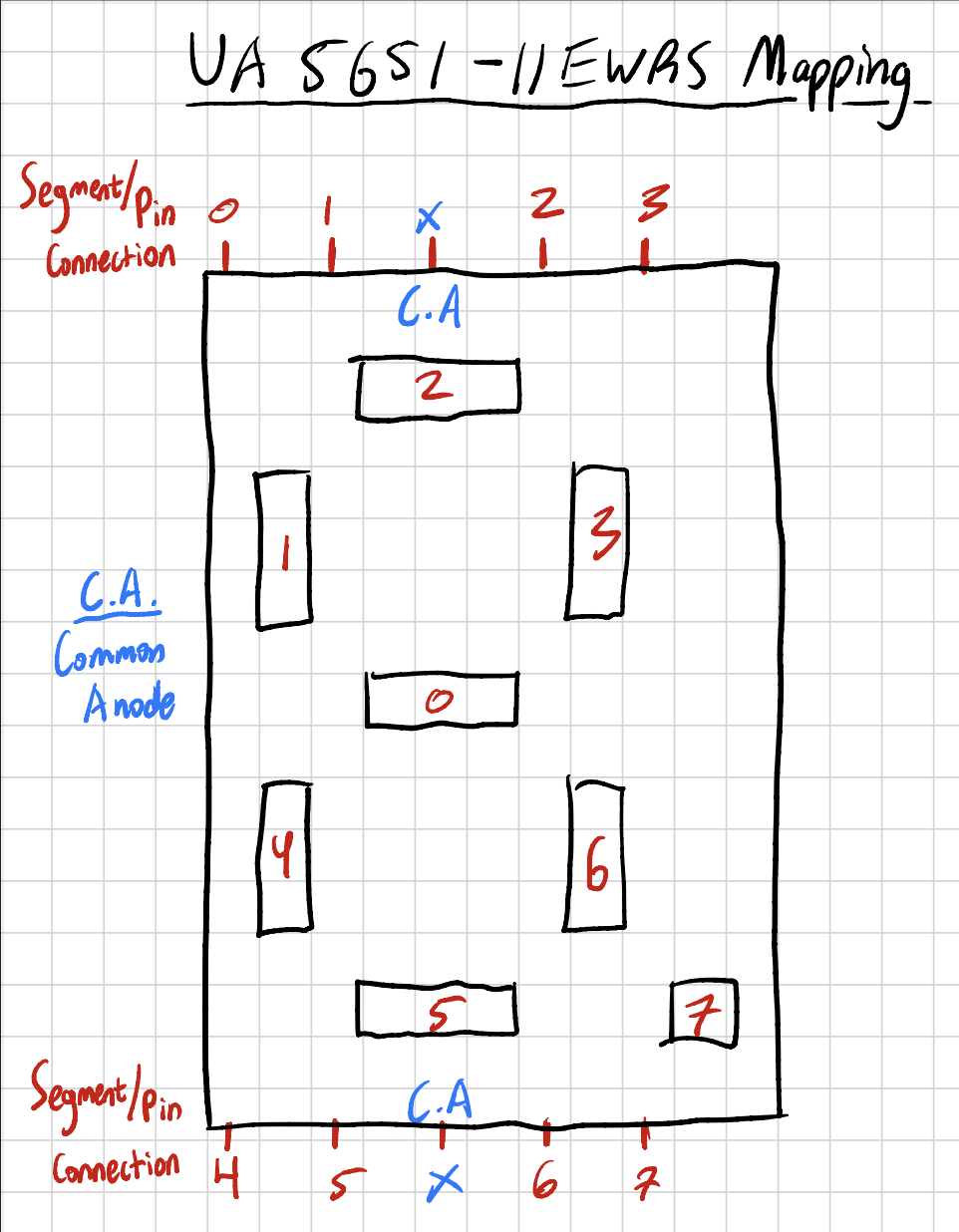
Note that this component uses a Common Anode, attached to the manufacturer’s pin 3 and pin 8 of the display. That is to say, by connecting my high voltage rail (in this case 3.3V) to either pin 3 or 8, it would supply the positive anode for every segment. The pins then could be controlled at logic high, leaving the segment off with 0V across it, or logic low, to supply the voltage differential which draws current through the segment and illuminates it. However, the forward voltage of these segment diodes is listed at 2.1V with a maximum forward current of 30 mA [see Jameco Datasheet]. Thus, in order to limit the current, as well as to bridge the remaining 1.2V gap between the positive rail and ground, a resistor needs to be added in series with the segment. In order to reduce the current load on my chip, I chose to operate the segments at a relatively low 5mA of forward current. Using this 1.2V gap and 5mA desired current, I was able to calculate a desired resistor value of 240 Ohms. Figure 3 below elucidates this point by supplying additional calculations and equations.
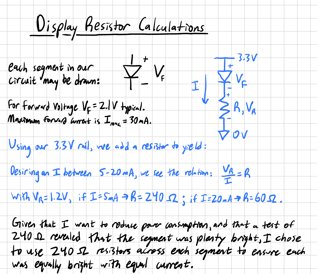
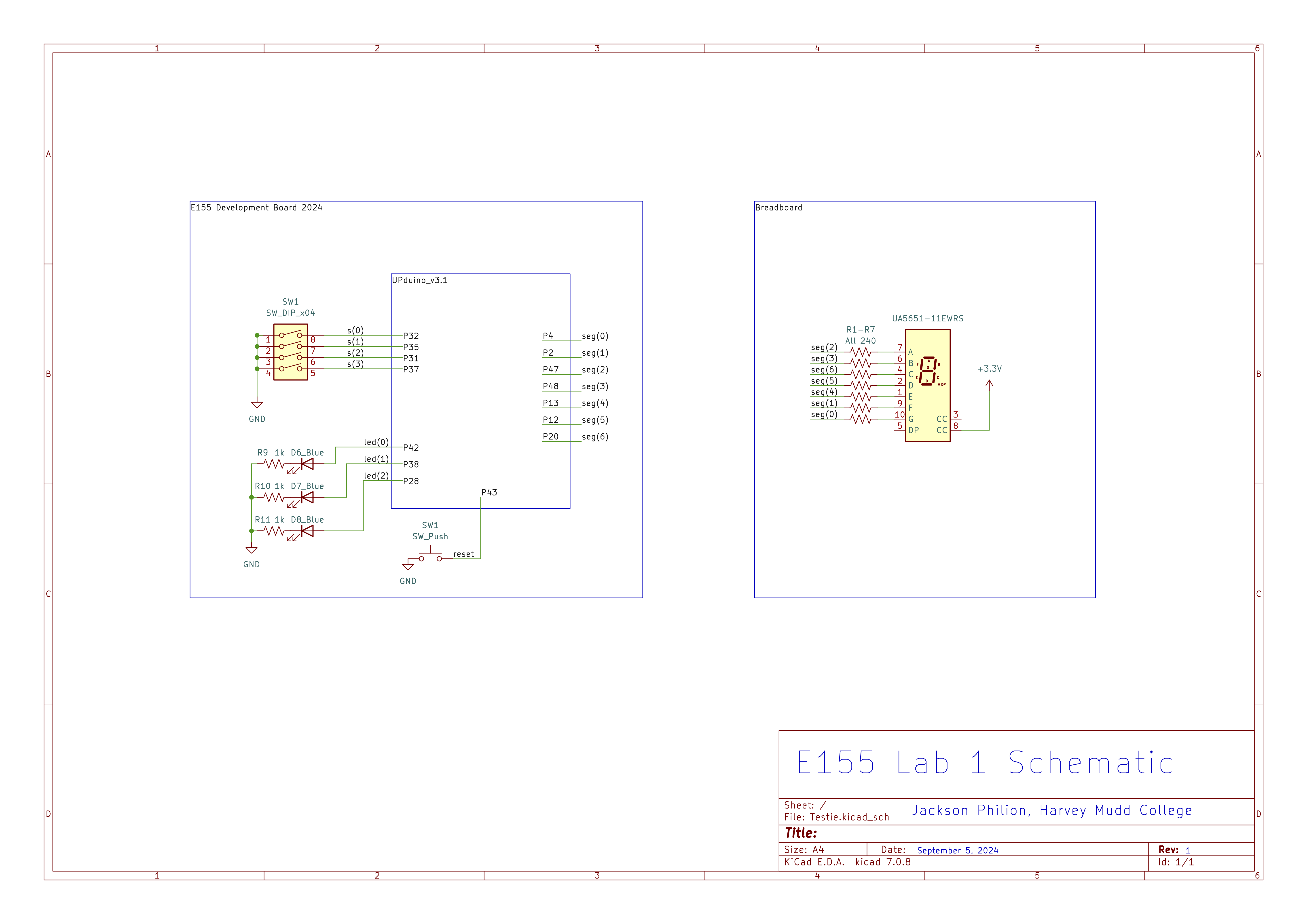
I chose to wire a resistor up to each segment in order to illuminate the segments equally brightly. If I chose to wire two segments up with the same resistor to ground, there would be no issue – the calculations might change, but with an operating current range between 5 and 30 mA, there is plenty of room to drive multiple segments with the same resistor. However, this would cause inequalities in current across the segments of the display, causing inequalities in illumination intensity. To maintain the same visible level of illumination, I thus opted to use a resistor for each segment I chose to illuminate. You can look ahead at the schematic I use down in Figure 6.
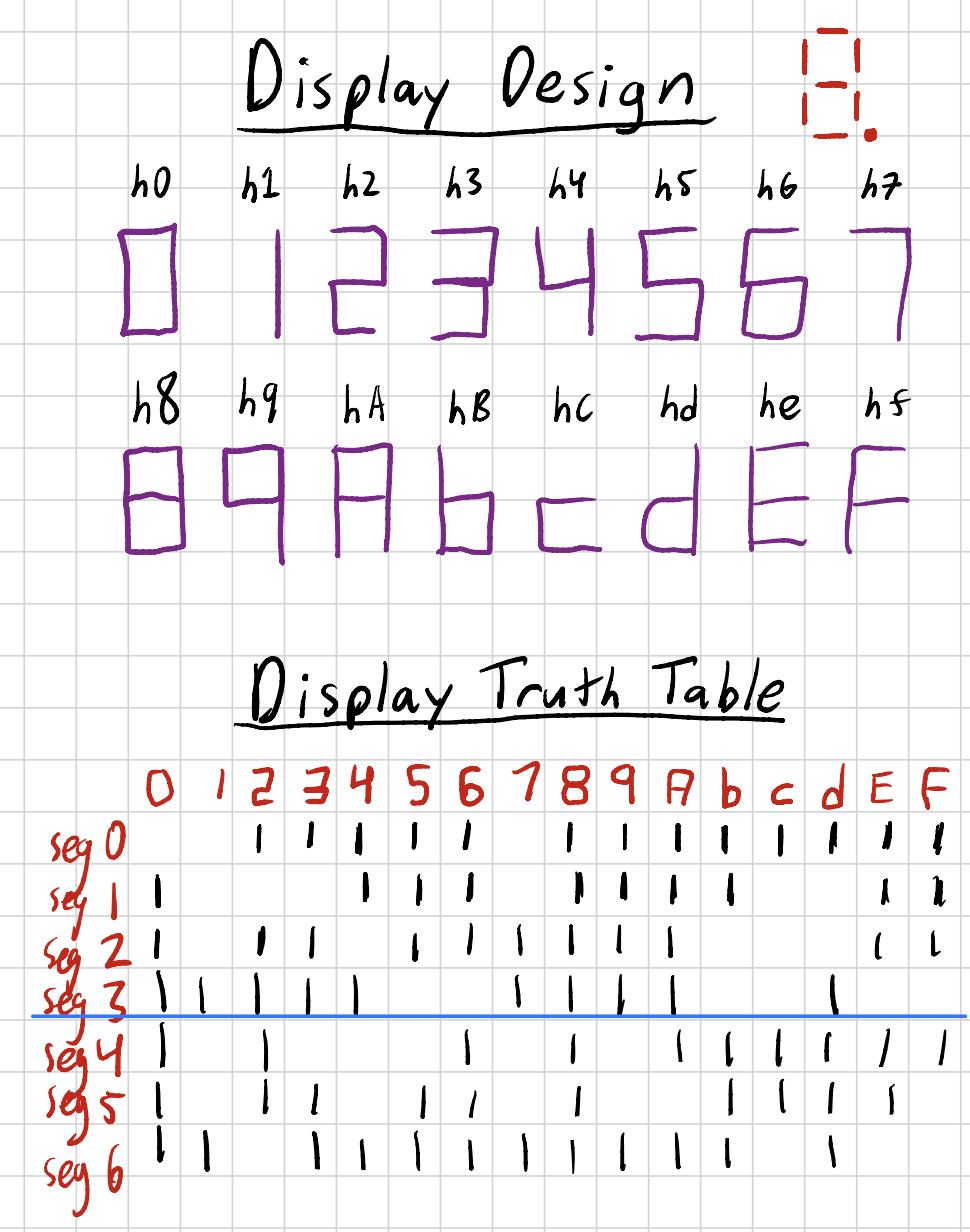
I finally had to decide how I wanted to illuminate the display to represent each digit. I first drew a design of each character as it would appear on the display, as seen in the upper portion of Figure 3 below. Understanding that I would need 7 lines of input to control the desired segments, I was able to determine that I needed an output signal of seg[6:0]. Using the digit design and these seg outputs, I then derived the truth table in the lower portion of Figure 4. This truth table allows me to describe exactly which signals need to be illuminated to represent each digit. Note a blank square is an implied 0, or “seg[i] off.”
Finally, there is the matter of the 3 onboard leds which should map to the oscillator and input switches. However, both led0 and led1 may be represented by simple “xor” and “and” operations in the FPGA, respectively. The final led2 output was dictated by an oscillator which similarly might be represented by an operation on the FPGA. None of the led signals required any external hardware that was not already onboard the E155 development board. Thus, I did not consider these outputs until I did my design in SystemVerilog.
Which is a perfect segue into the next section! Having understood the functionality of the display, the circuitry I needed to construct around it, and the truth table I wanted to implement, I finally had to consider how I would use the FPGA to generate my seg[6:0] and led[2:0] signal outputs using SystemVerilog language.
System Design
I had most fun in this lab with the system design in SystemVerilog. It was always one of my favorite pieces of E85 Digital Electronics, and this held true for this first lab of E155. Figure 5 below describes the abstract view of inputs and outputs that my SystemVerilog modules are based upon.
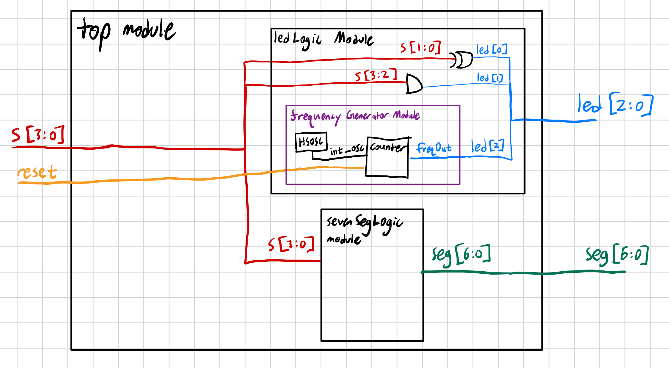
Using this diagram, I began to build out my code in SystemVerilog. You can find my .sv code files at in by Lab 1 github repository here.
Additionally, you can find the final schematic in Figure 6 below. Note that I hooked up my breadboard pins first at my convenience, then went back after the fact and used Lattice Radiant to assign the pin outputs. This schematic also shows how I hooked the seven segment display up with the common anode and separate resistor for each segment.
Simulation
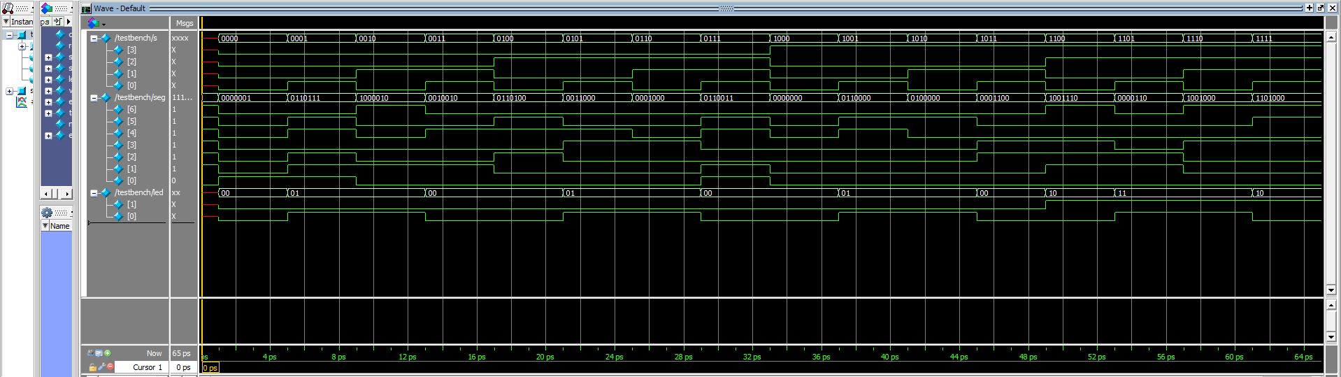
After writing my code, I endeavored to simulate its proper function using ModelSim. Note that I would have wanted to use the Questa simulator built into Lattice Radiant, but licensing issues left me using the good old desktop app instead. I first ran a series of forces to set my inputs and verified that each output read as intended. The results of this may be seen in Figure 7 below. Note that the raw image may be viewed, along with the source code, at my Github here.
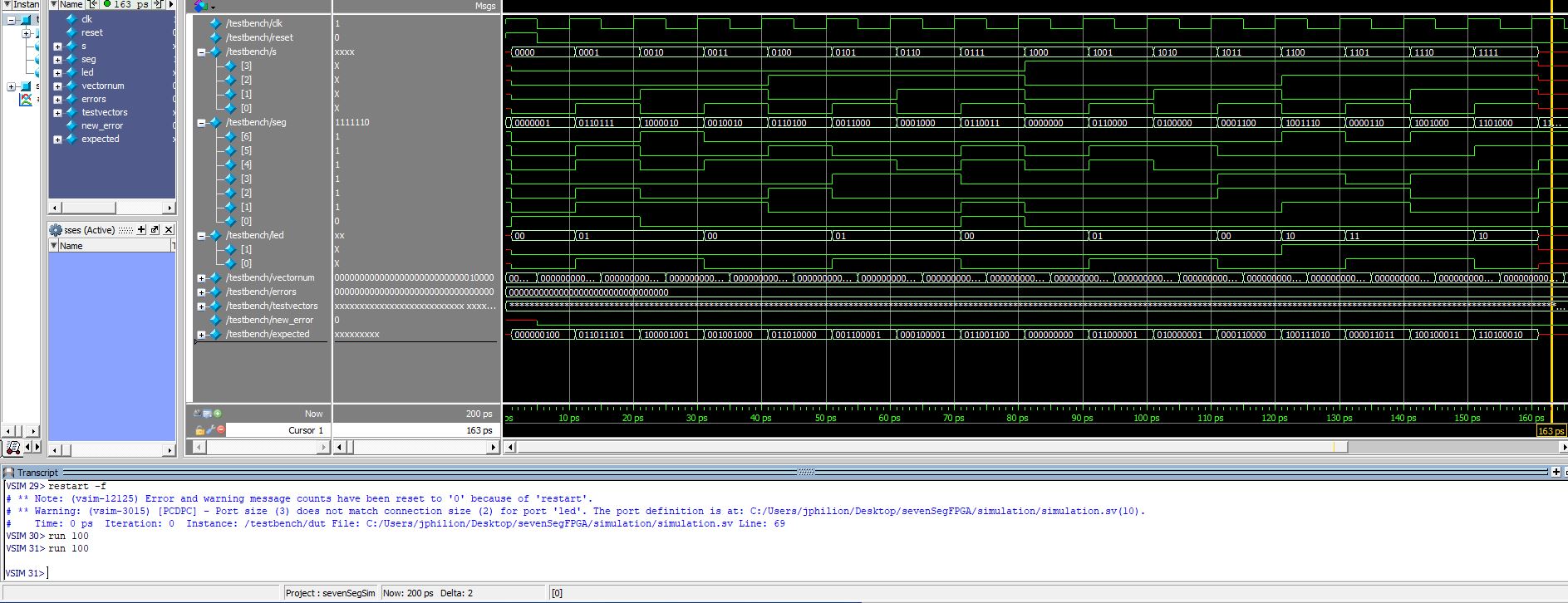
However, I wanted to stretch myself to write an automatic testbench instead. I believe that this skill will be instrumental for my SystemVerilog going forward, and I wanted to dust off my testbench-writing-chops right away. After many attempts (and finally removing the .txt extension from my .tv file), I was successful! It does not yet run automatically, needing instead to be fed the command “run 163” after simulation start. Yet, the test bench displays zero errors across each test case (which was all of them). It loads and evaluates each test vector from the .tv file. I am incredibly pleased, and aim to jump off of this first test bench in order to write my next one for lab 2. The successful run results may be seen in Figure 8 below, yet again, the raw image may be found on my github here.
Completed System
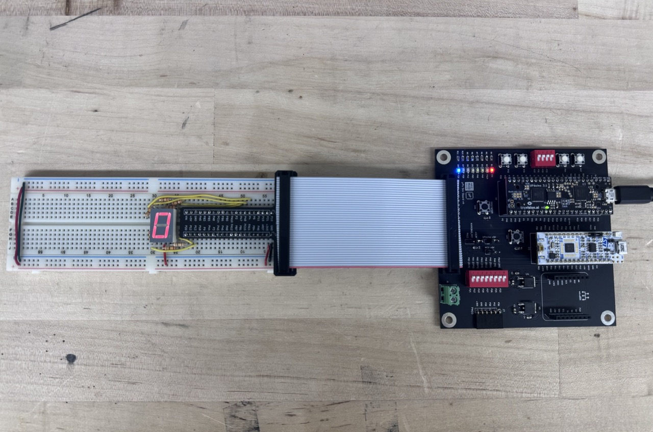
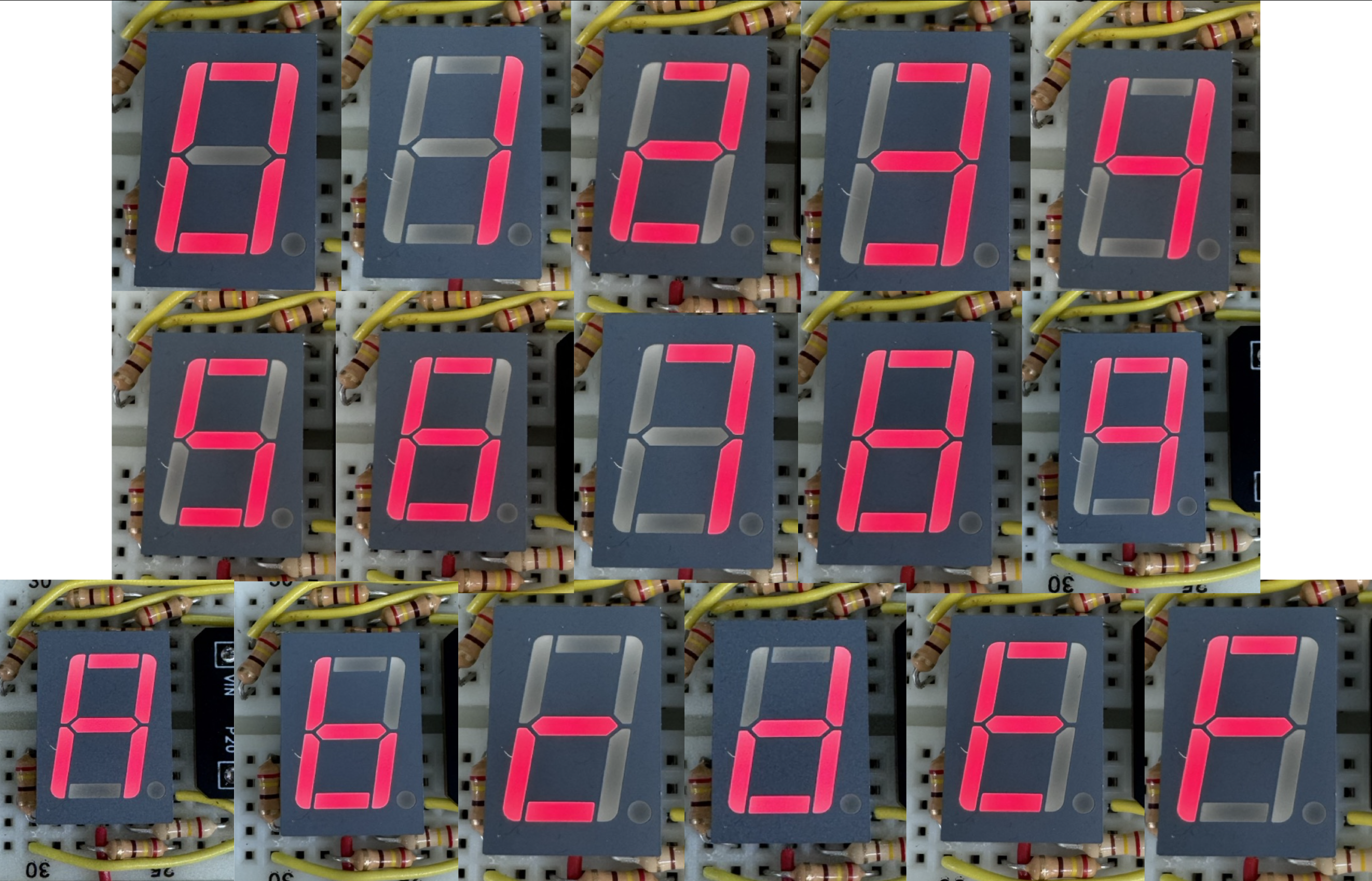
Finally, with a system designed and tested, I prepared to upload it to my FPGA. I ran into multiple errors on one particular lab computer with programming. While the computer could detect the FPGA and the linking cable, the connection would fail when trying to run the final step. However, after switching to a new computer which a friend had used successfully, I was able to download the code to my system and demonstrate its success! The LED system worked as intended. I did not carefully clock the frequency of led[2], intended to be 2.4Hz. It was certainly doing between 2-3 cycles per second, so I assumed that it was working as intended. However, next time, testing this more thoroughly may reveal further issues for investigation – hard to say without nailing down a measured frequency. However, back to the success! Below you can find Figure 9 with the full system shown, as well as Figure 10 demonstrating that the seven segment display responds as intended with equally bright segments.
Thus concludes my interactions with Lab 1. You can find a reflection of this weeks work in the blog postings, or can head on over to Lab 2 and see what’s next! Spoiler alert: We’re going to try and double the amount of displays without doubling the GPIO burden.