Quick Stats
Time Spent: 21 Hours, 35 Minutes, 14 Seconds
Misunderstood Ideas: 1
Resulting Unnecessary 3D Prints: 1
Resulting Unnecessary Wiring Harnesses: 2
Testbench: Automatic
Dual Display: Steady, Discrete, and Illuminated
Overall: Success
See my Blog Reflection for more! Dare I say, it contains a particular treat this week.
Lab 2: Multiplexed 7-Segment Display
Lab Task: Double the Display
For the unfamiliar, Lab 1 asked students to read in a set of 4 switches, representing a hex number from h0 - hF. Lab 1 already set up the system to display this number using a single seven-segment display and a set of onboard LEDs.
Lab 2 asks students to build on this system by adding a second set of switches which control a second seven-segment display, and to use LEDs to instead display the sum of the two 4-bit switch inputs as a 5-bit number. Here’s the catch – the lab challenges students to accomplish this doubling in display capacity without instantiating a second module in SystemVerilog, and without using a second set of FPGA pins. In other words, students were tasked with doubling the display outputs without doubling the hardware.
Enter: Time Multiplexing
We can use time multiplexing to accomplish our double display task. Time multiplexing gives designers a way to utilize common hardware for different inputs and outputs. For example, in a high speed processor, having a unique data line going between every part inside would waste space and be expensive. Instead, designers create a shared pathway, letting different units use it to communicate at different times. I think of it like a landline in a time before cell phones – not every member of the family needs their own. You can install one for the whole house, then schedule a time for each family member to make their calls. Voila, you have time multiplexed your house! Take a look at Figure 2 below. Here, you see a block diagram illustrating the idea, as well as a timing diagram describing how one might lay out the signals in time.
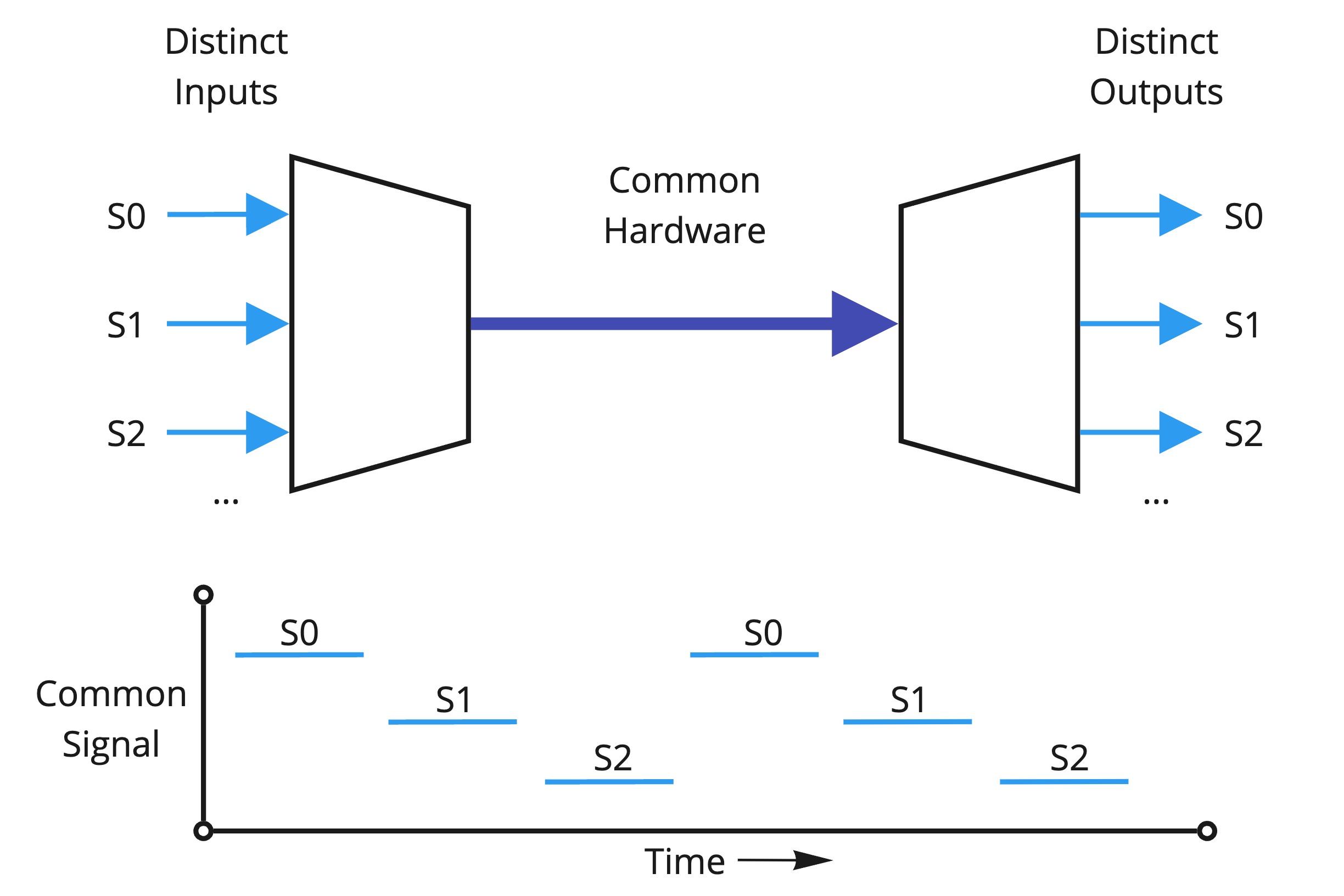
In this case, we have two sets of input switches which want to use the same limited FPGA pins to illuminate their displays. Luckily for us, the human eye isn’t too great at detecting flicker. The United States National Institute of Medicine reports that humans cannot distinguish between flashes of light if the time separating them is less than 10 milliseconds, or over 100 Hz – they will just see a solid glow. On the other hand, our FPGA has an internal oscillator capable of running at 48 MHz, nearly a half million times faster than our eye can detect. So, if we simply use the same set of pins to control either display, turning one on and then the other in sequence, we can easily create the illusion of two simultaneously powered displays while using the same hardware to control them. In my case, I chose a frequency of 500 Hz to be extra safe.
Hardware – Understanding and Setup
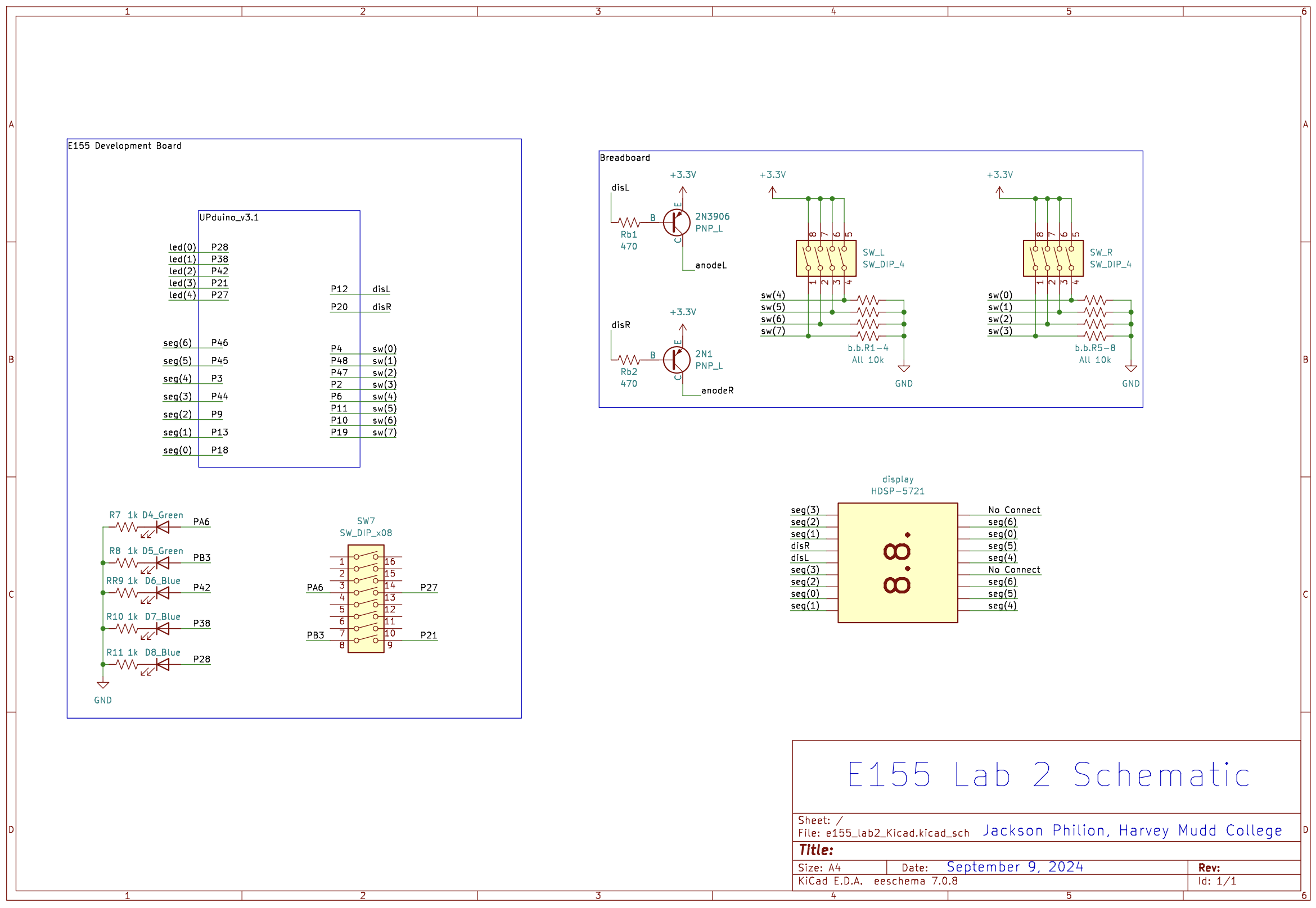
The hardware for this lab required a few special considerations. First off, we used a different seven segment display. It still had a common anode schematic, but I instead used a dual display with the following pin mappings as seen in Figure 3 below:
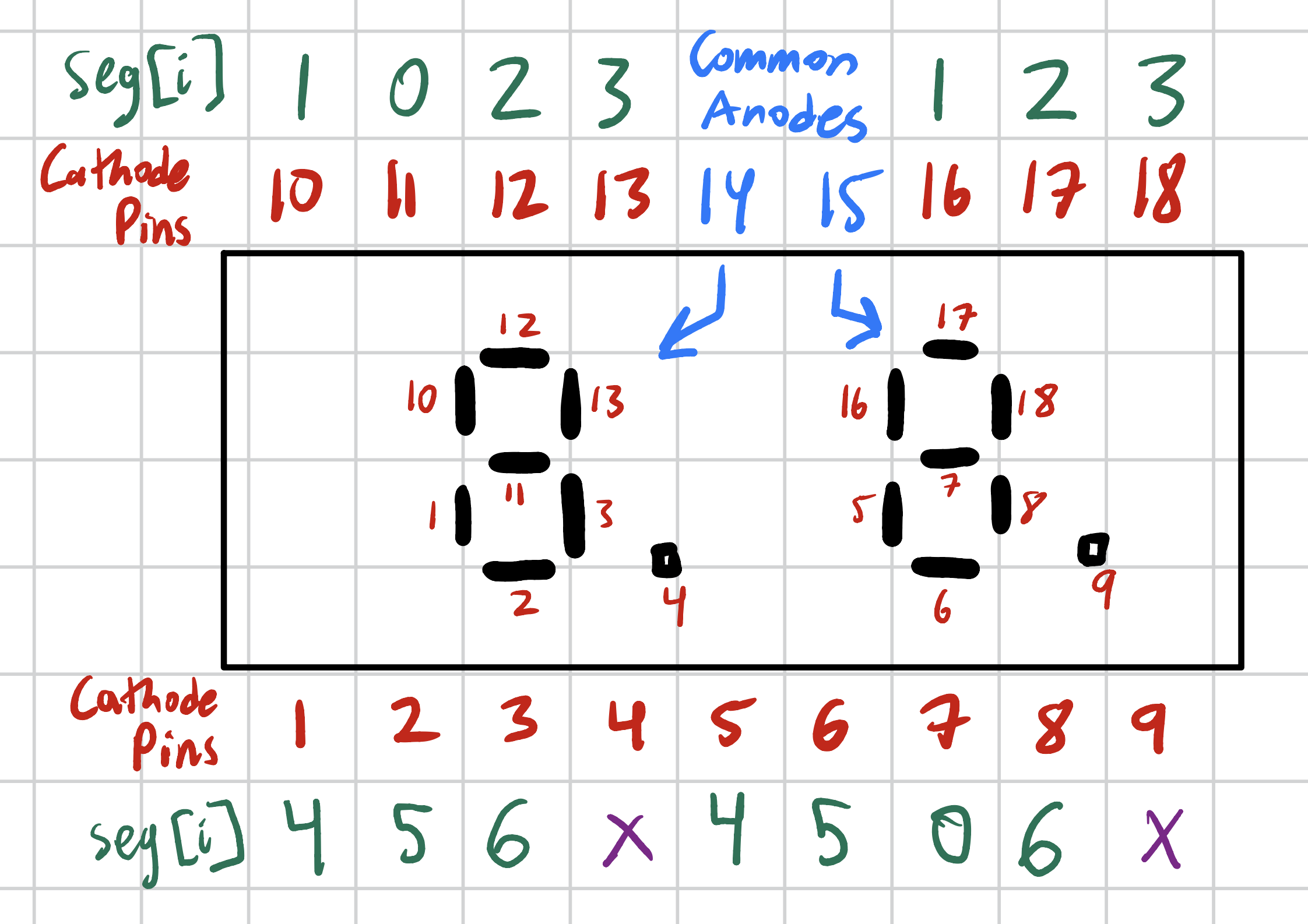
I was able to use the same calculations from Lab 1 to show that a load resistor of 240 Ohms is sufficient to limit the current to under 10 mA for each segment – recall the maximum is 30 mA. Now, note in the figure above that there is a common anode for each side of the display. That is to say, two connections to power should be made in order to illuminate each half. This is where I may apply a time multiplexing scheme. I can control which display gets powered at any time, making sure that I ground the other anode, in order to effectively switch between the two displays. By doing this at my chosen 500 Hz frequency, the human eye will interpret both displays as solidly on. Then I can run the same seg[6:0] signal to the display pins on both sides. By switching the digit I send down these shared segment pins, and lining these changes up with the L and R power signal, I can effectively control two displays at once with the same 7 lines of segment hardware (plus two power control signals).
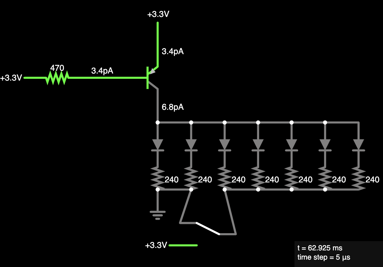
However, I now need to configure the common anodes to be controlled low or high via my FPGA pins. One might ask – couldn’t you just use the FPGA pin directly to control the voltage level? The answer is no – the segment draws an unsafe amount of current, too high to be routed directly though the FPGA pins. Specifically, this datasheet about our iCE40 FPGA chip indicates that at 3.3V logic, the maximum I/O current is 8mA. Given that I draw just under this with a single segment, I cannot use it to control the common anodes. Instead, I may use a PNP transistor switch. The simple circuit and calculations which describe its behavior may be found below in Figure 4. In summary, a base resistor of 470 Ohms allows our FPGA pin to control a single point, Vin, to enable to disable each pin. In this process, the maximum current allowed in the transistor pin is limited to 5.5mA, an acceptable maximum. Also note that my diodes should be pulling between 5 and 8 mA, similarly under the FPGA pin current limit, per my Lab 1 calculations.
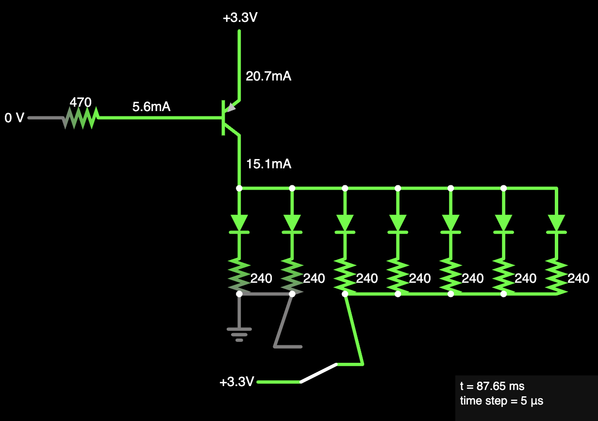
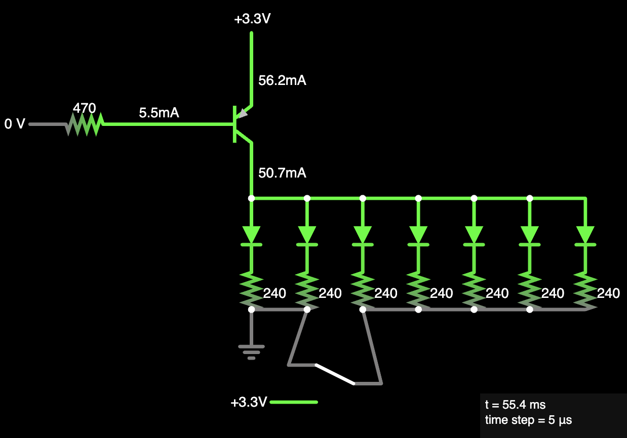
However confident I was with this design, I wasn’t sure how it would interact with a varying load. Recall that each number displayed illuminates a unique sequence of LED segments. Displaying a 1 requires illuminating 2 segments, while displaying an 8 requires illuminating all 7. I wasn’t sure how this varying load would affect the current though the FPGA pin and LED segments, even if I was relatively confident that I had designed my system to operate at the maximums. So, I turned to Flastad, an online circuit simulation tool, to help me understand how my circuit would respond to different illumination regimes. The following Figure 5, Figure 6, and Figure 7 show the three different operational minimums and maximums of the circuit – illumination off, illumination on with a minimum display load, and illumination on with a maximum display load. In each case, we see that the current through each LED segment into the FPGA pins, as well as the base current, is well within specificaiton.
Finally, I considered how I would chose to display the 5 LEDs which represented the sum of both 4-bit switch groups. I decided that I could use the 3 blue LEDs onboard the E155 development board, the same as those used for Lab 1, while also using the two green LEDs above. These could be connected to the FPGA using the fourth and eighth switch on the board’s SW7 8-pole DIP switch.
With my connections determined, I created a breadboard circuit according to the following schematic in Figure 8 and proceeded to design my software. Note that the schematic may also be found in PDF form on my Lab 2 github here, under notes and extras.
Software – Block Diagram & SystemVerilog
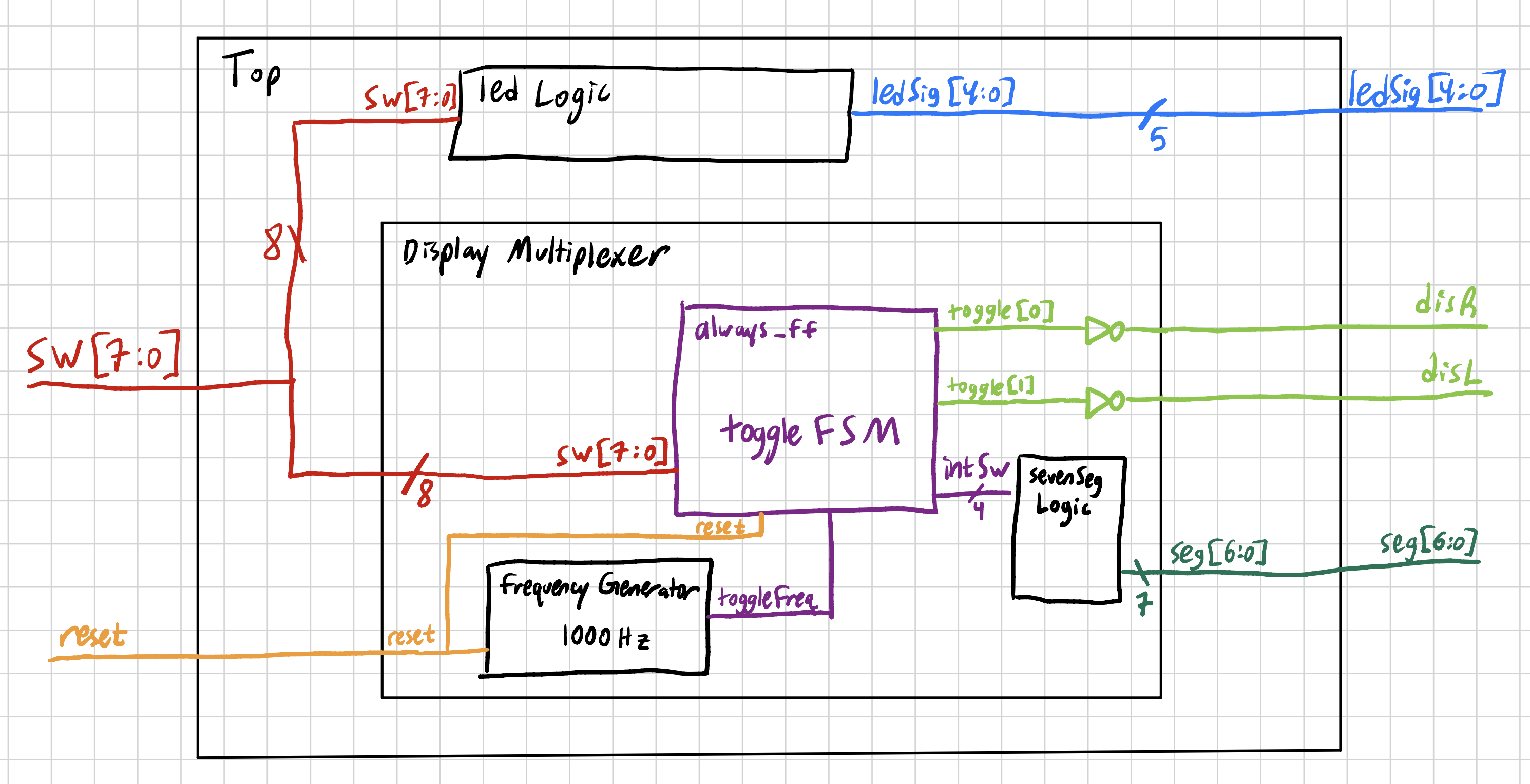
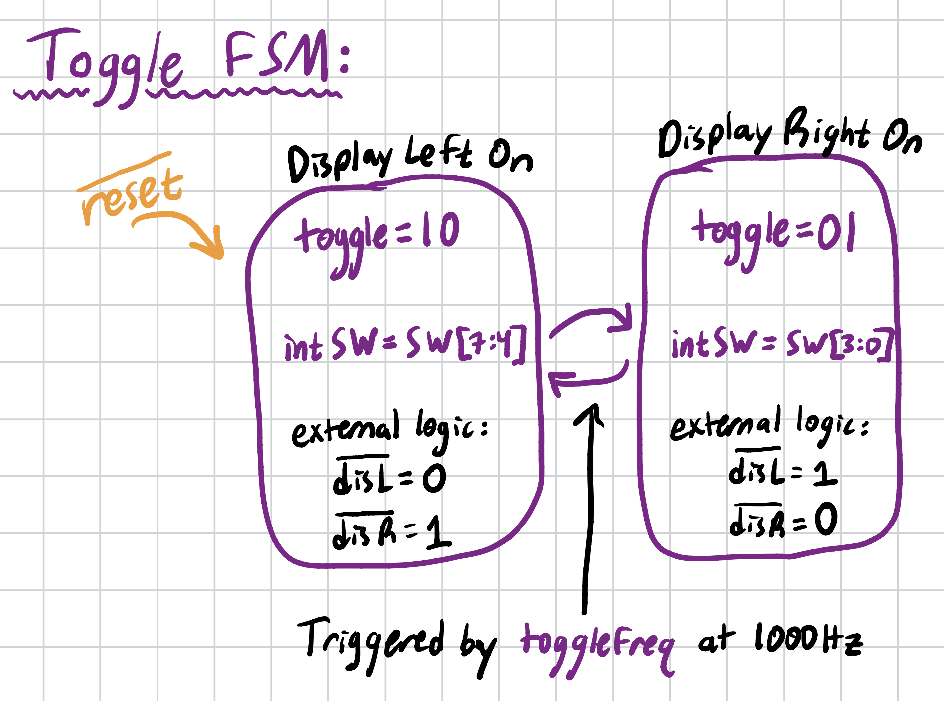
Having designed the hardware, I proceeded to plan out my software implementation. I first created a block diagram to describe my system, as found in Figure 9 below. Note that I included a sort of Finite State Machine, or FSM. Well, a quasi-FSM. At the very least, something that is best described by a Moore FSM diagram. In this case, I wanted to switch between two states, displayL and displayR, at a chosen frequency “toggleFreq”. Since I want the display to flash at 500 Hz, I set the toggleFreq to 1000 Hz since the switching nature of the FSM effectively halves the toggleFreq. This diagram, in Figure 10, describes the Toggle FSM block in Figure 9.
With this understanding laid out, I proceeded to write my SystemVerilog code. This may be found in the FPGA folder on my Lab 2 github here. Aside from some debugging trying to pass parameters to my frequency generation module, it was relatively smooth sailing.
Simulation
For this lab, I was easily and effectively able to write a testbench to demonstrate that my LED logic. The testbench code may be found on my Lab 2 Github, and the waveform and successful run message may be seen in Figure 11 below.
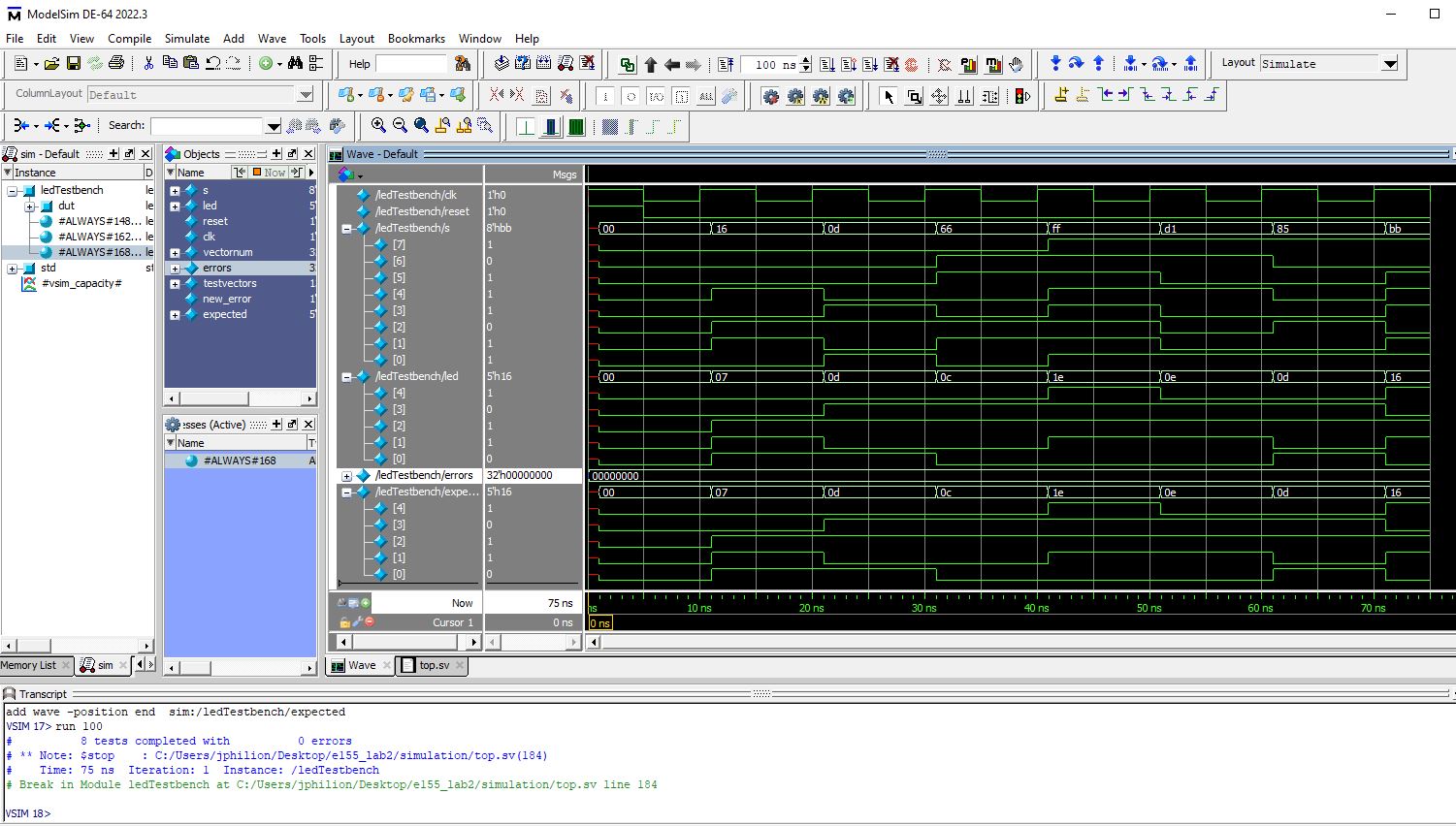
Recall that lab 1 already demonstrated (by automated testbench) the successful functioning of the seven segment logic module. Similarly, I have demonstrated that my frequency generator module is effective, and I continue to use/reuse it in this lab with a different frequency parameter.
The tricky module to thoroughly test in an automated bench is the displayMultiplexer module. For this, I decided to use a hybrid manual/automatic testbench. I removed the internal oscillator and frequency generator from the module, and instead passed in my own toggleFreq line. I chose to simulate this signal at a rather rapid pace, letting me easily see whether the display was switching or not in simulation. The automatic part of the testbench involved using a .tv file to load in my switch inputs and to generate waveforms of my expected illuminated outputs. The manual part of the testbench involved checking the results. I basically ran the toggle signal out of sync with the testbench’s internal clock, meaning that I wouldn’t be sure what to read out, when. Instead of finagling the two signals to sync up, I decided that manually checking was both easier and more effective. Figure 12 shows my view of the whole simulated testbench, including the 4 test points. For these test points, I chose to display 00, 06, C9, and F3. I figured that if these all displayed the right segments, and the display signal toggled as expected, then I could demonstrate the module was working. Figure 13 shows a close up example of one of my test points, as well as some marked analysis that demonstrated my thinking.
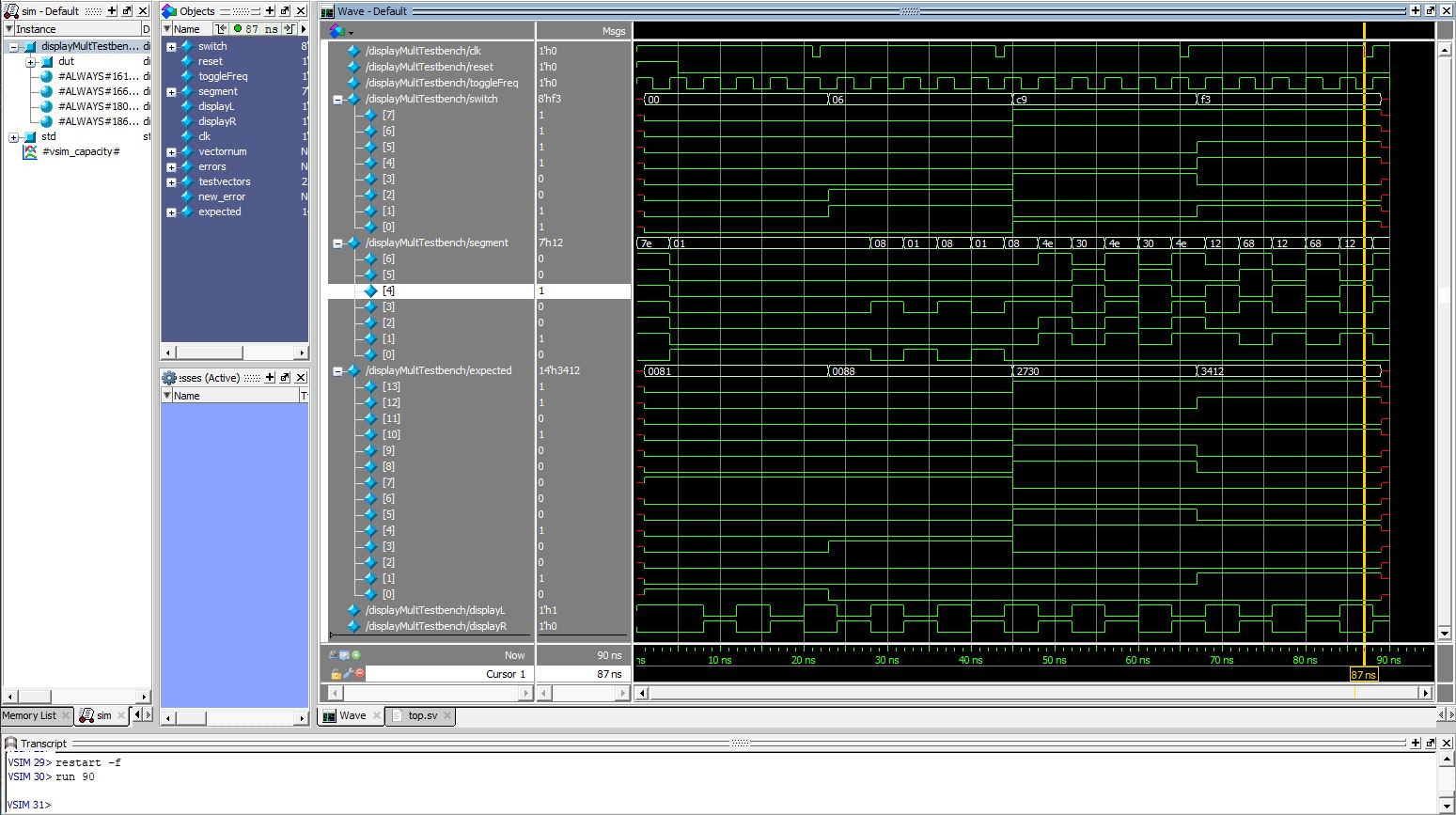
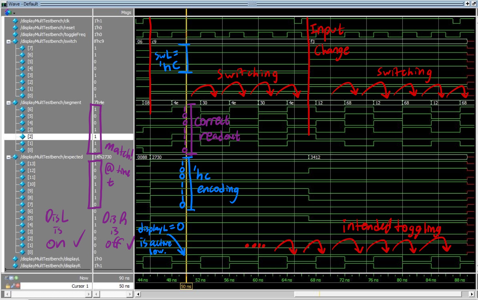
Note that these images may be found also in the extras folder of this lab’s Github here. In any case – all signals generated as expected! Testbench success for all modules!
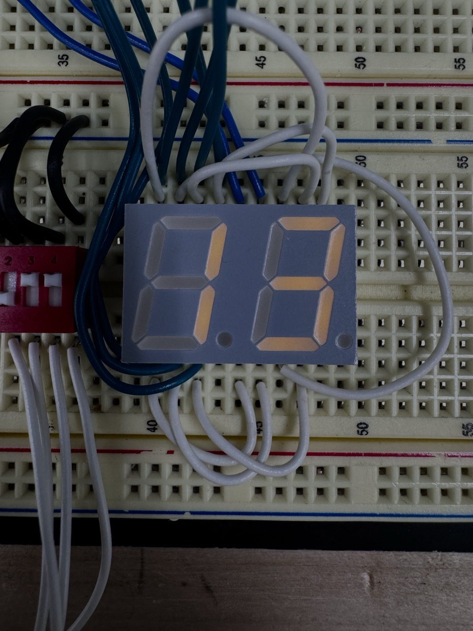
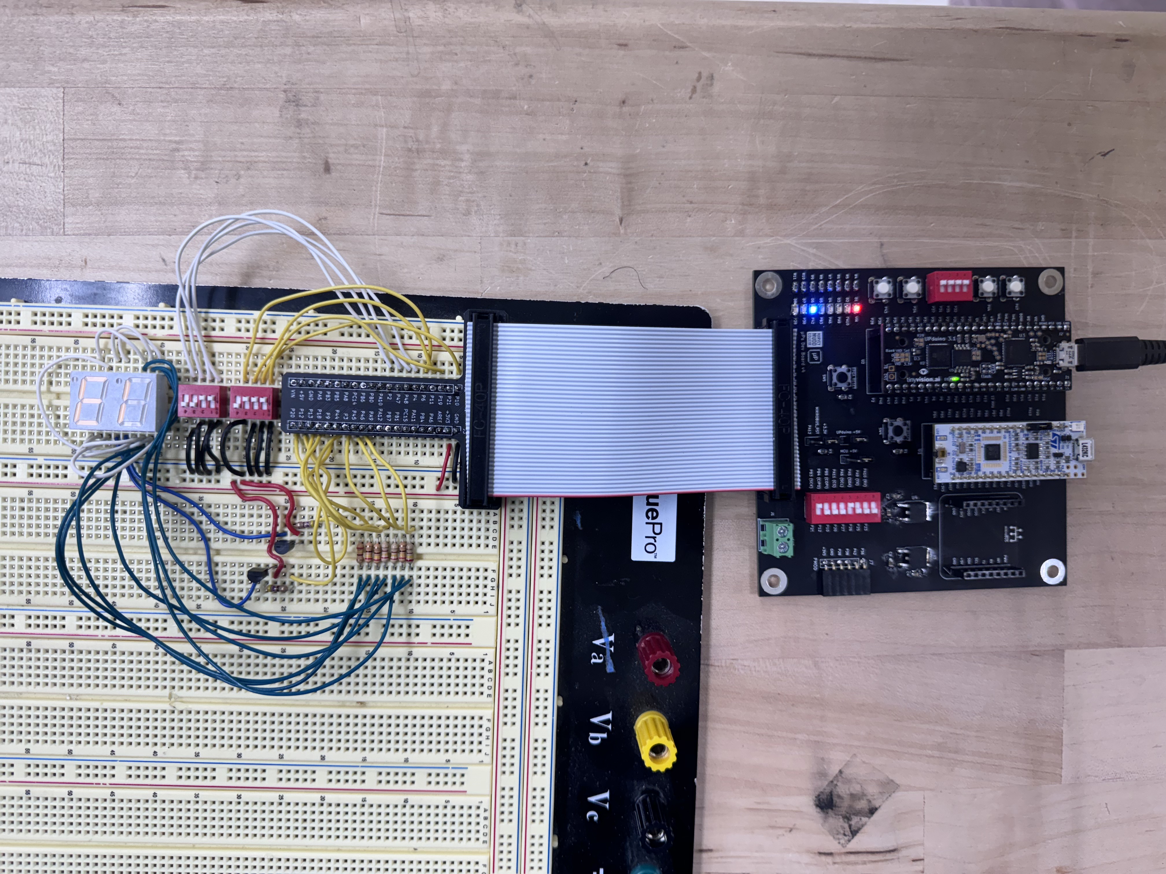
Final System
After assembling the final pieces together and running the programmer, the system worked as expected. The display itself was a touch dimmer than I may have liked – I think part of the problem was the color I chose. I could have boosted the current values to get a brighter display, but as Figure 4 showed, I had already thought carefully about my tolerated currents and did not wish to push my luck. Thus, I yield my full system, shown in Figure 14.
A final reminder that full images, source code, and more can be found in this lab’s Github here. In addition, to learn more about the mysterious “Misunderstood Idea” and “Unnecessary” 3D prints and wire harnesses that I mentioned in the top stats, check out my blog post for this week! So much work gone to… well, not waste, but… to the blog post! Until next week.