Results
This section first contains a report on all of our projects specifications, describing which ones were met as-is and which ones were modified or un-met. Then, this section provides the simulation and logic analyzer results which demonstrate successful operation of portions of our system. Finally, this section concludes with a presentation of the final system and its capabilities in the form of images and videos.
Overall Performance
First, see below for a list of our original project specifications when we first proposed the project:
As we accessed the success of our final system, we reformatted and adjusted the above list of specifications for clarity and accuracy. See our final report on specification status below:
Simulation and Logic Analyzer Results
As we constructed the HDL code to control the LCD display, we found it helpful to use the simulation tool ModelSim to generate test waveforms of our system’s inputs, internal signals, and outputs. Through this process of iterative debugging and testing, we were able to finally generate the following figures which demonstrate a successful system:
In the above image, we were looking to see whether the system would default to a waiting state without the need for an external reset to prime the system. The above waveform shows that the low level FSM correctly defaults to s0_powerup, while the mid level controller FSM correctly defaults to wait_SPI. All other signals are as expected, though they are not particularly relevant at this point.
In the above image, we are checking to see if the system properly holds steady until a SPI transaction has completely finished. After completion, we are checking to see if the system correctly stores the sent number, and correctly converts it to a letter and a number representing the corresponding note. Then, we are checking to see whether the system correctly starts the display sequence. We see all of these objectives are met!
In the above image, we are checking to make sure that the system executes the proper mid level controller FSM sequence, sends the intended commands as a final output to the LCD, and displays the intended character and letter. We see a resounding final success!
Additionally, we were able to verify these outputs using a Saleae Logic 8 device and the associated software Logic 2. The following image shows a successful initialization and powerup sequence between the LCD unit and our FPGA:
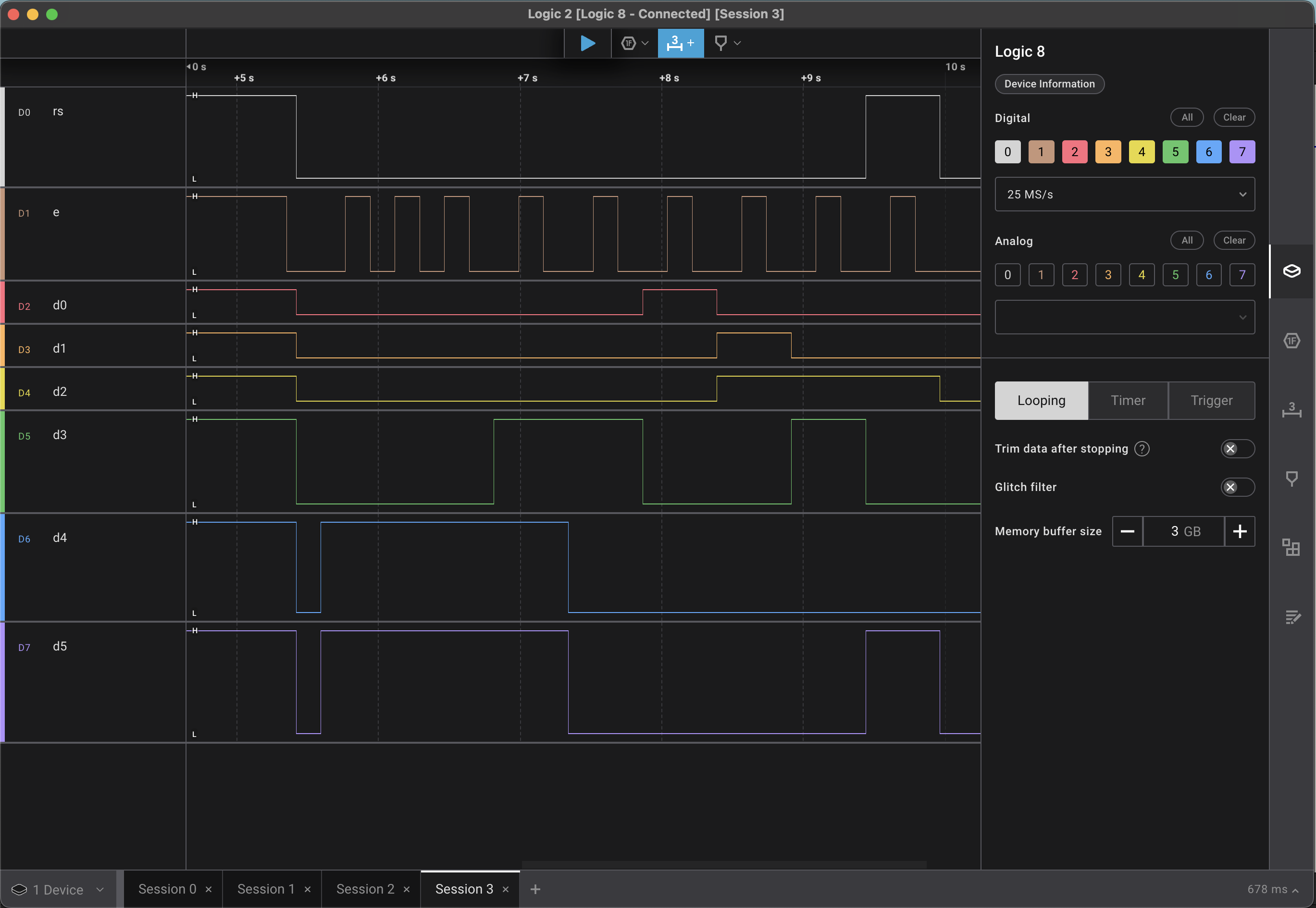
We correctly see the sequence sending 9 commands by tacking 9 distinct enable pulses. We see rs properly staying low until the final command, and by tracing the state of D0-D5 (note that D6-D7 did not fit on the scope, but should read 0 for the first 8 commands), we see the correct instructions sent each time. Note that the instructions should mirror the following sequence:
d[7:0] = 0011 0000, rs=0, Function Setd[7:0] = 0011 0000, rs=0, Function Setd[7:0] = 0011 0000, rs=0, Function Setd[7:0] = 0011 1000, rs=0, Configured[7:0] = 0000 1000, rs=0, Display Offd[7:0] = 0000 0001, rs=0, Cleard[7:0] = 0000 0110, rs=0, Entry Mode Setd[7:0] = 0000 1100, rs=0, Display Ond[7:0] = 0111 0100, rs=1, Write “$”
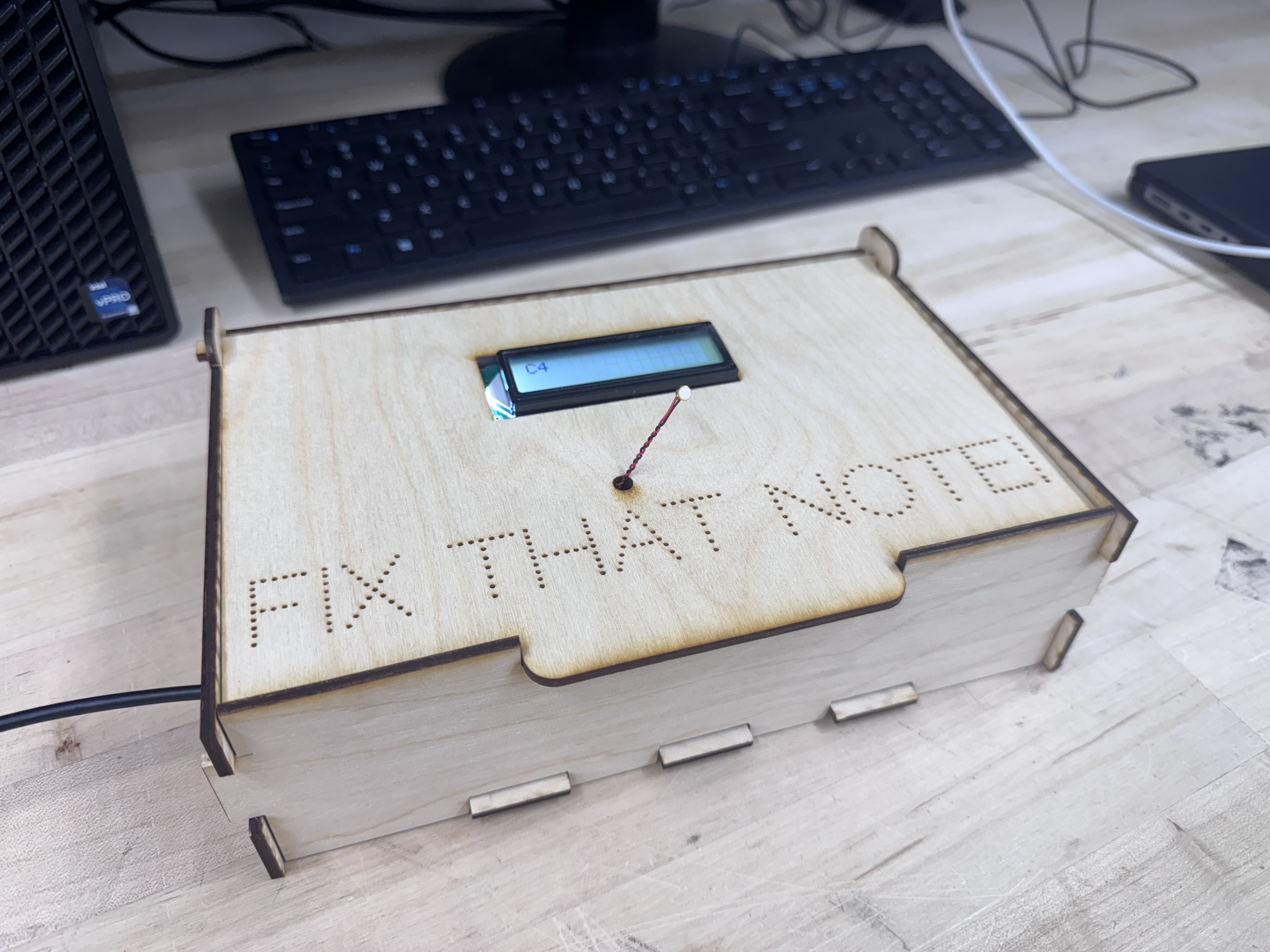
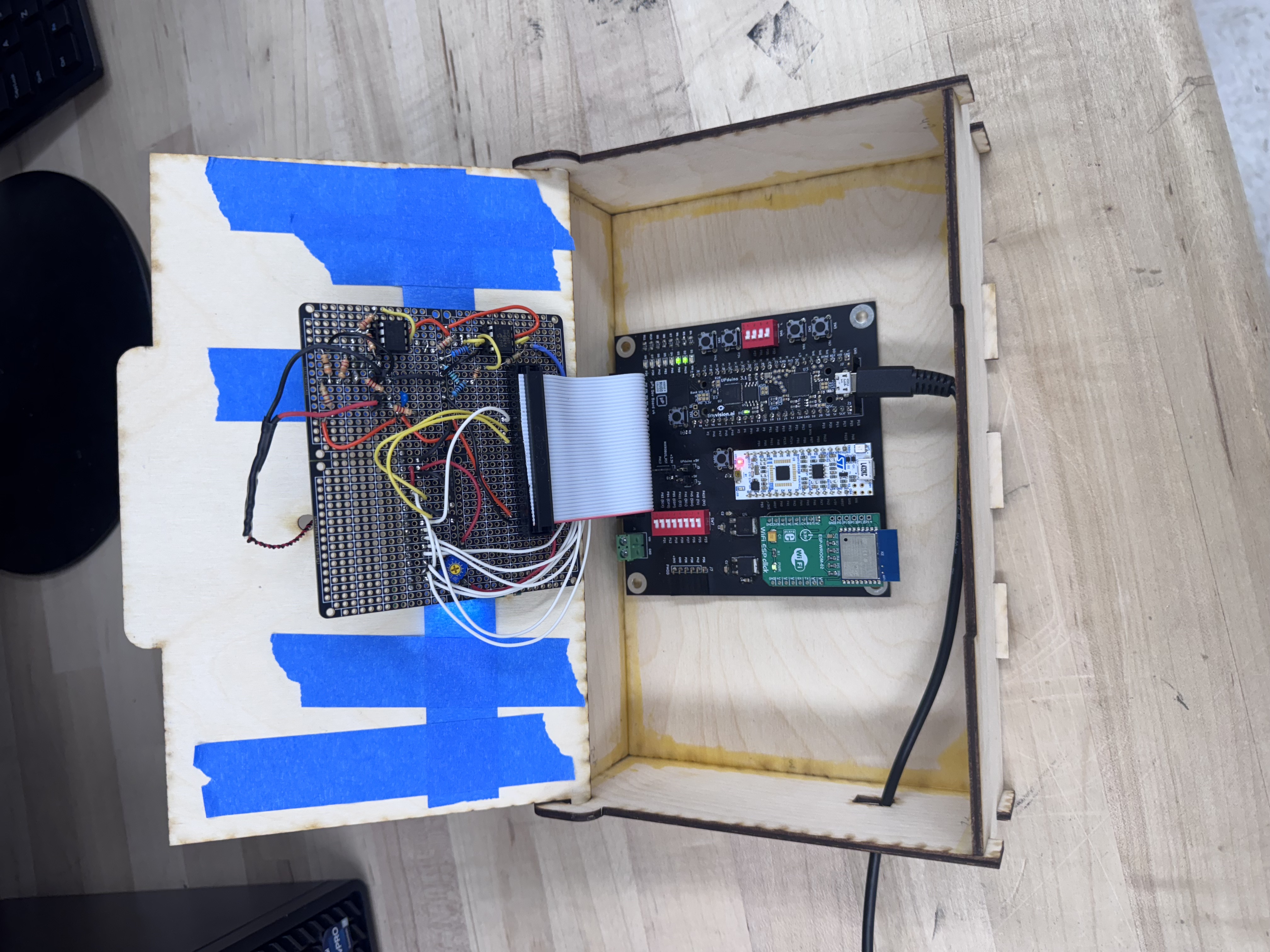
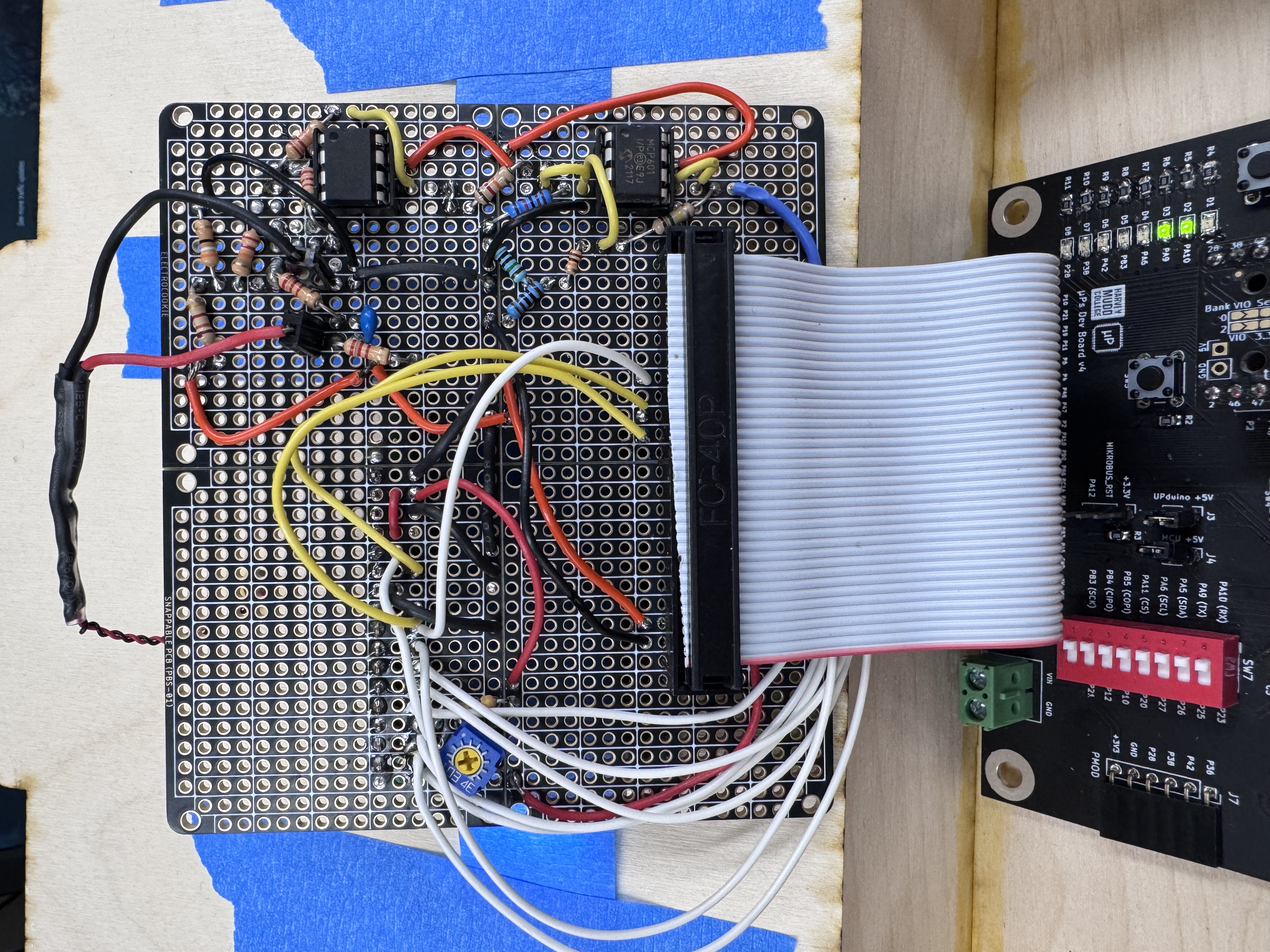
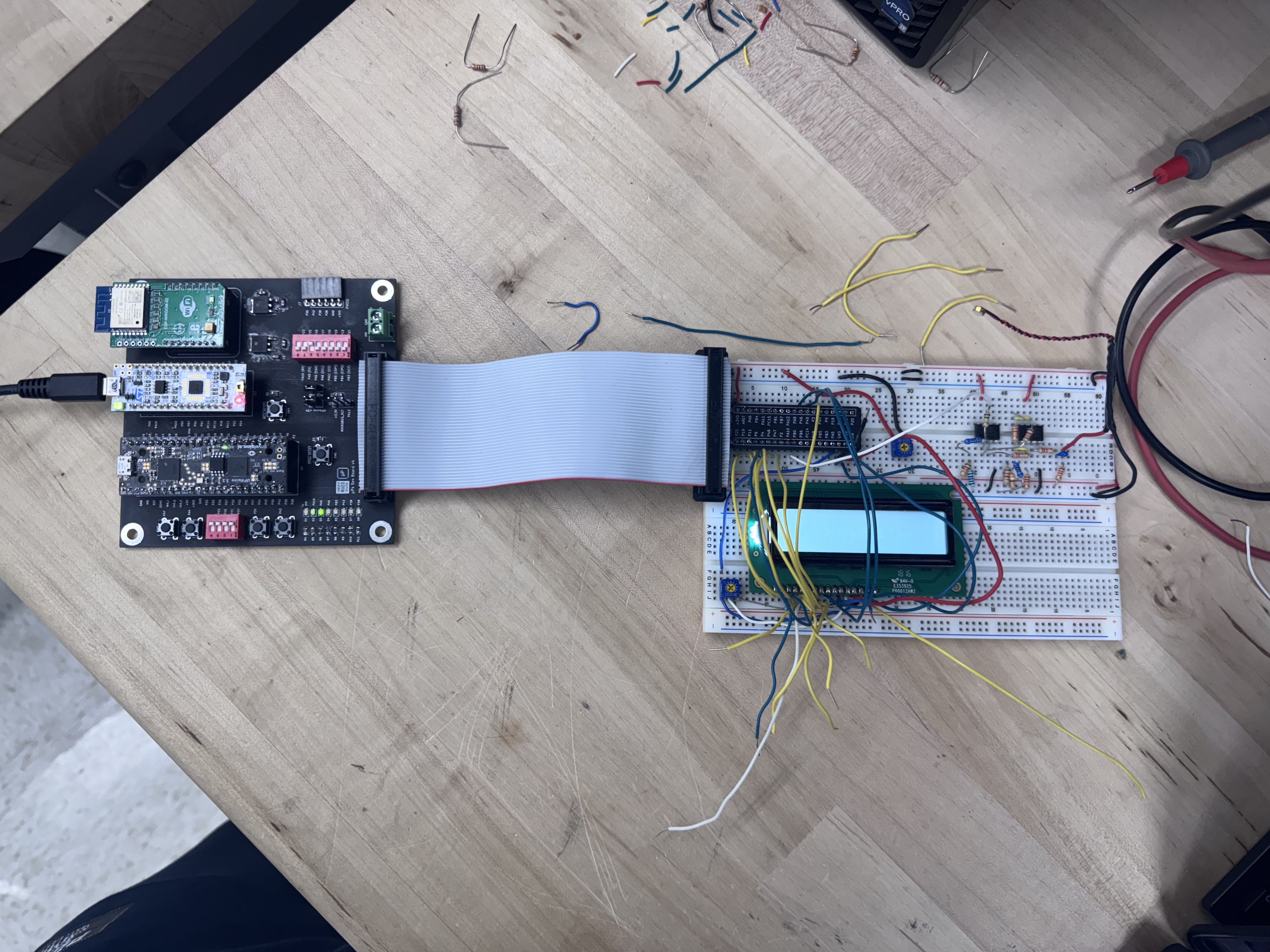
Final System and Full Demonstration
