MCU
Summary
The project uses an STM32L432KCU microcontroller to process audio data. To do so, it needs to enable three key elements: the ADC peripheral, the DMA peripheral, and the CMSIS DSP library. To communicate this data with the external LCD driver, the MCU must also interface with its SPI peripheral.
ADC
The ADC digitizes the sound waves captured and amplified. The DMA facilitates direct data transfers to the memory without the CPU’s involvement. Using the DMA ensures real-time data acquisition, as is suitable for frequency analysis. To configure the ADC, the ADC clock is enabled through Reset and Clock Control (RCC), and a GPIO pin (PB0) is set to operate in analog input mode. The ADC is calibrated for optimal performance, and configured for 12-bit resolution, 6250 Hz sampling rate, and continuous conversion mode.
DMA
The DMA is configured to transfer data from the ADC data register to the memory. The DMA clock is enabled through RCC and DMA channel 1 is assigned to handle data transfer. Both memory and peripheral data size are configured as 16 bits for the 12-bit data, and circular mode is disabled to ensure the data in the memory will not be overwritten before frequency analysis is done.
FFT
For frequency analysis, the CMSIS-DSP library is implemented to perform Fast Fourier Transform (FFT) on the audio data. Before performing the FFT, a Hanning window is applied to the data to reduce spectral leakage, improving the accuracy of frequency calculation. The FFT output is analyzed to determine the dominant frequency by identifying the peak magnitude in the frequency spectrum.
SPI
Finally, the calculated frequency is transmitted to the FPGA via SPI. SPI is configured to transmit the frequency data as a 16-bit value.
Dual Buffer Design for Audio Data Processing
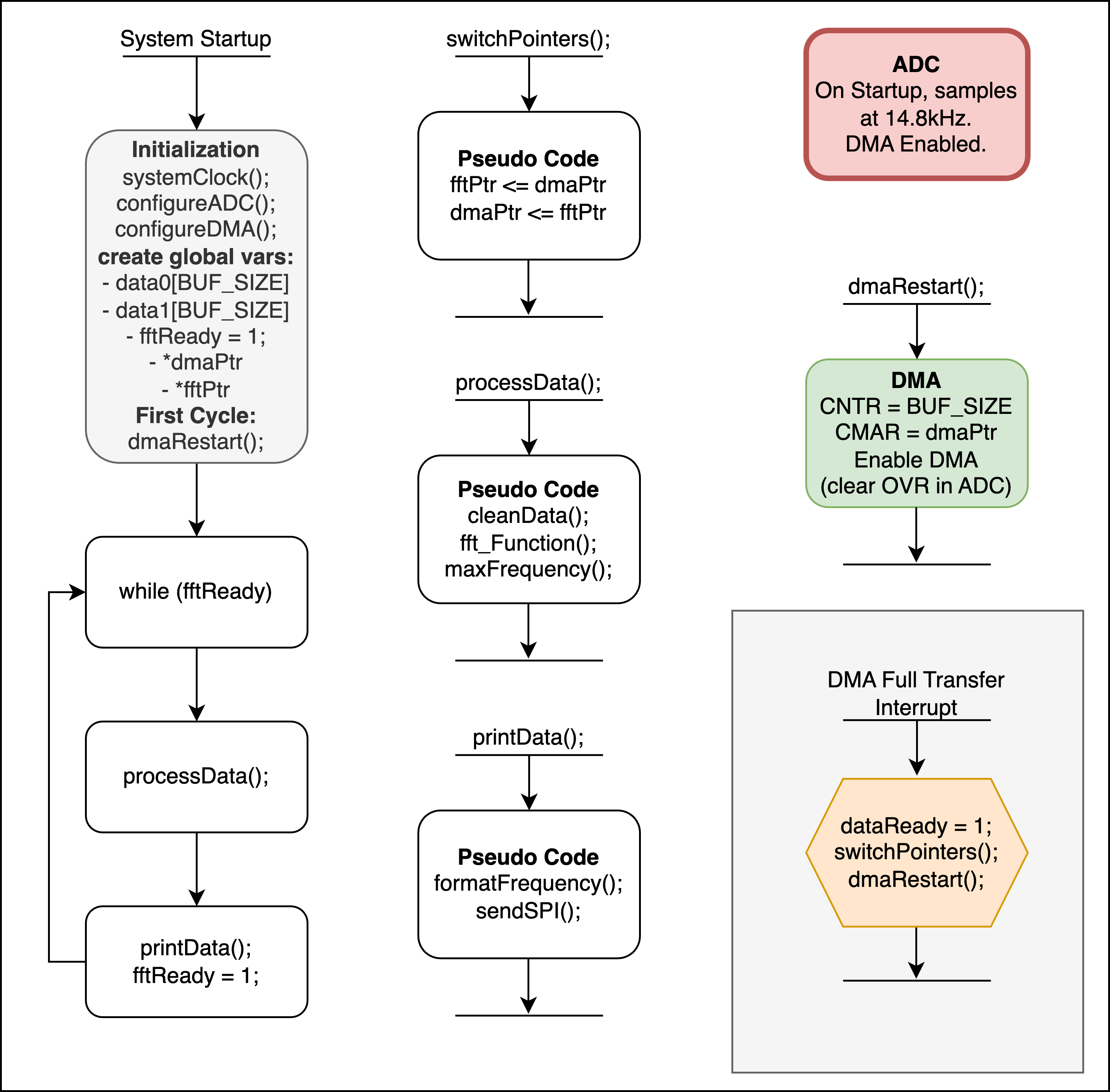
To manage continuous audio data acquiring and processing without interruptions, a dual buffer design is implemented. The design uses two buffers (buffer1 and buffer2) in the SRAM alternatively for DMA data writing and FFT data processing. While DMA writes to one buffer, the other is processed by FFT. This design avoids data loss or overwriting during FFT processing, as the two operations can occur simultaneously and independently.
Initially, the buffer1 is configured as the target buffer for DMA to write ADC data, while buffer2 is idle. This setup ensures that the system has a clear starting state.
Once the DMA completes transferring a full buffer of ADC samples, it triggers an interrupt, handled by the DMA1_Channel1_IRQHandler function. In this interrupt service routine, the system performs two critical tasks. First, the interrupt status flag is checked to confirm the transfer completion. This flag is then cleared to allow the system to respond to subsequent DMA interrupts. Second, DMA is temporarily disabled to safely update its memory and control configurations, ensuring no conflicts during buffer switching.
Before switching buffers, the handler checks if FFT processing has completed on the previously filled buffer. This is done using a flag (FFTReady). If the FFT function has not yet processed the buffer, the interrupt handler exits early, allowing the processing to catch up.
Once FFT processing is confirmed to be complete, the system alternates the roles of the two buffers. If buffer1 was being used by the DMA to collect data, it is now assigned to the FFT processor, while the DMA begins filling buffer2. Conversely, if buffer2 was the active DMA buffer, it is swapped with buffer1.
After the buffer switch, the DMA settings are updated to reflect the new buffer being used. The memory address pointer for the DMA is updated to point to the new target buffer (DMAptr). The buffer size counter (DMA1_Channel1->CNDTR) is reset to ensure the DMA knows how much data to transfer in the next cycle. The ADC overrun flag is cleared to avoid potential data corruption errors, and the DMA channel is re-enabled to resume operation.
After the buffer switching process, the handler resets the FFTReady flag, indicating that the newly filled buffer is not yet ready for FFT processing.
System Diagram
See a diagram of our microcontroller routines in the figure below:
