FPGA
Summary
In order to control the LCD screen, which is described in detail within the New Hardware section of Documentation, we chose to create a system of nested FSMs. The following sections describe both of these FSMs in detail, as well as outlining the HDL modules we used to connect the whole system.
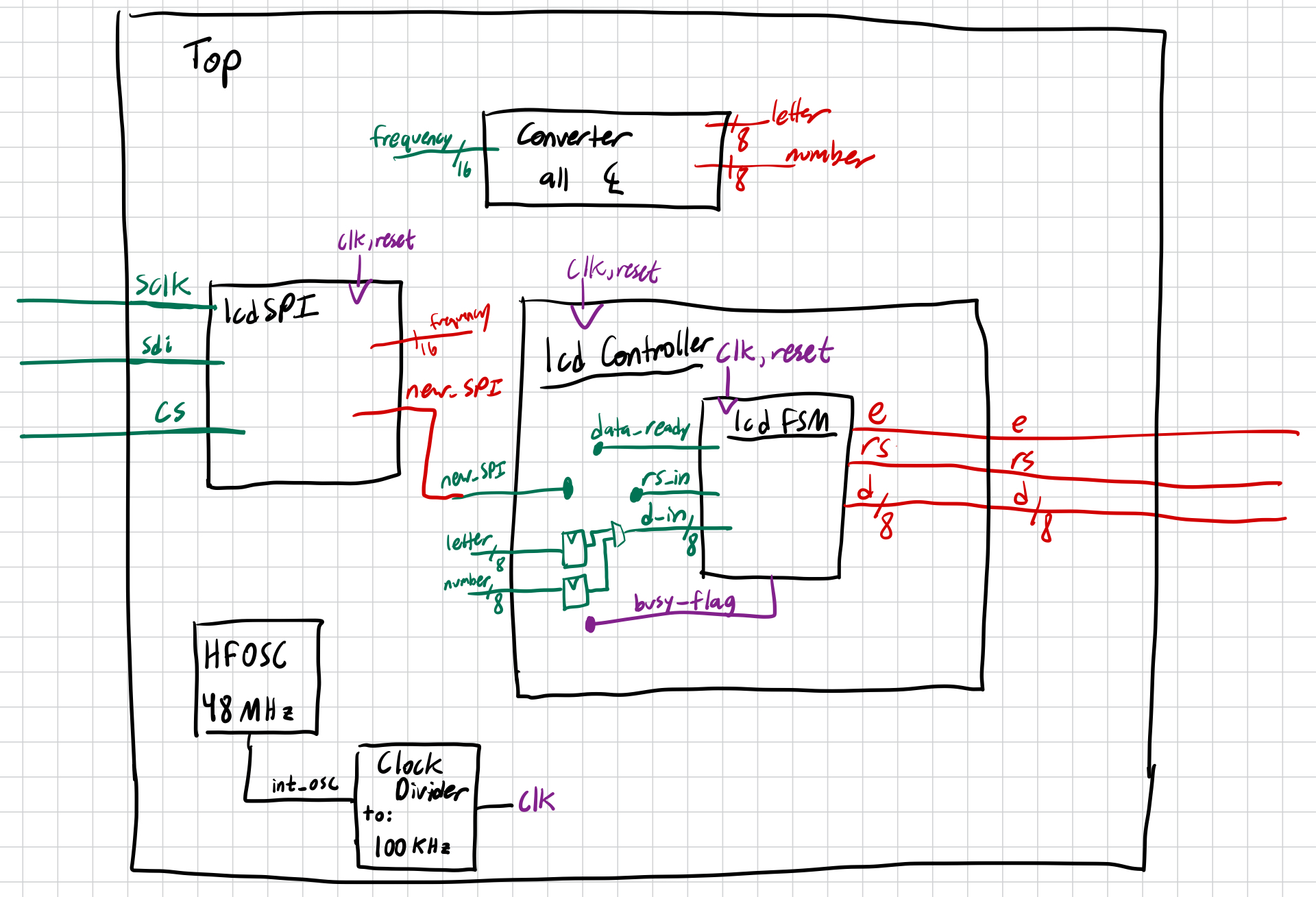
I first created the following hand drawn block diagram to outline the modules that I would need to control the LCD and SPI system.

From this design, I identified 5 key modules to make:
- A top module, to contain the oscillator and clock divider parts of the system
- A low level FSM, for the LCD’s control of individual commands
- A mid level controller, to control the order of commands sent to the low level FSM
- A converter module to switch from frequency to pitch notation
- Finally, a SPI module to store the incoming data and regulate the system’s response to incoming SPI transactions.
Top Module
Overall, our top module had prescribed inputs and outputs. We need this unit to read in the SPI data from the MCU, and output the 10-line parallel interface data to control the LCD. The highest level block diagram, describing all the interconnections between the modules described below, may be seen here:

Note that this module was almost entirely a connecting module, containing very little logic. Yet, it does have two key things aside from basic module interconnects. Firstly, this module directly contains the call which instantiates the high frequency oscillator (HFOSC, 48 MHz) and adds a clock divider (which outputs a final frequency of 100 kHz). Secondly, this module contains some unpictured debug logic which can be hooked up to any signal at any time to read out the current state of the system for debugging purposes.
Low Level FSM Module
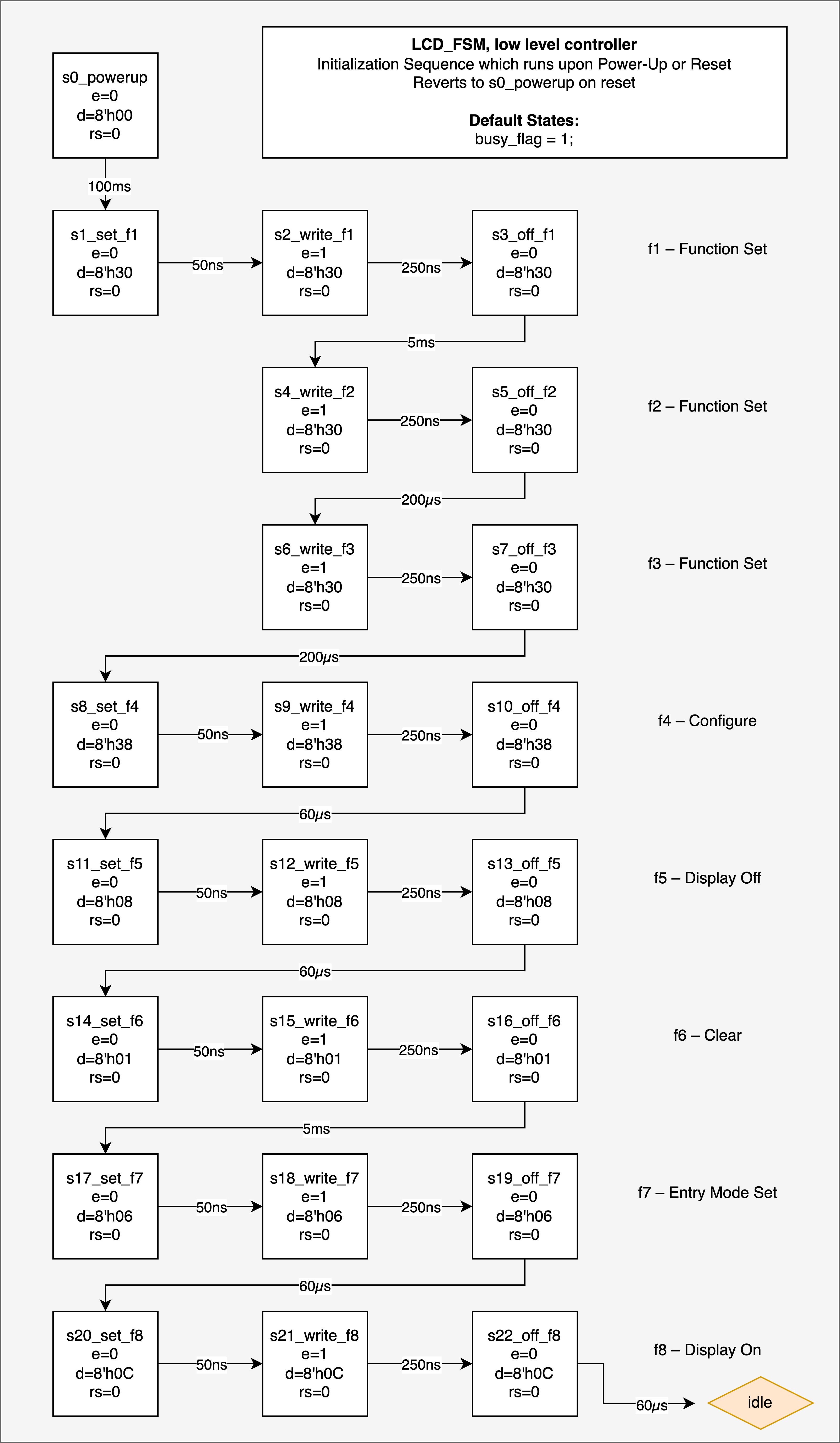
Our low level FSM module is responsible for directly controlling the data, rs, and enable lines. This module specifies the timing requirements between signals, and contains the programming which ensures that the system initializes properly upon system powerup or reset. In order to accomplish this initialization sequence, we first created a 22 state FSM to control the timings and instructions necessary upon restart. The state diagram is shown in the figure below.

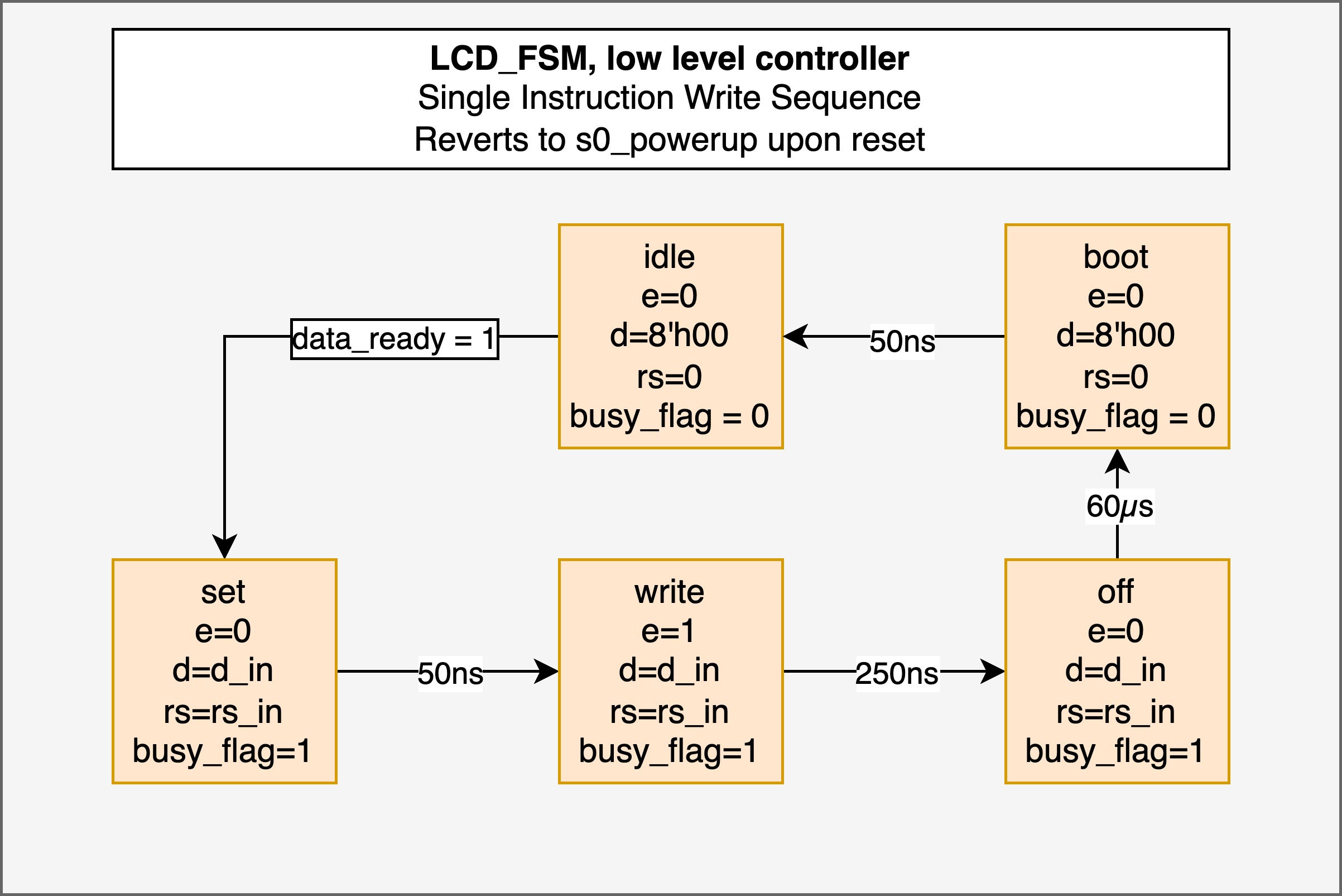
In order to track the system timings, we used a main counter and a series of flags that set themselves as the counter reached the appropriate time mark. Each time the state transitioned, or state!==nextstate, the counter and flags all reset to 0. This allowed us to track time in a repeatable and simple way throughout any state we needed to time. Finally, note that the system enters into an idle state. Since this state differed so significantly from the rest of the initialization sequence, we chose to represent it as a separate FSM shown in the figure below. Note, however, that this FSM is a part of the same module as the initialization sequence above.

This is the main loop of our low level module, if one considers it like a microcontroller routine. The default state of the system is to powerup and then wait for an incoming instruction to write a new command. However, this fsm only manages the timing between transactions and writes single commands. In order to control which instructions should play in which order, we created a separate mid-level FSM to isolate the system which sends commands from the system which dictates the order in which to send commands.
Mid Level Controller Module
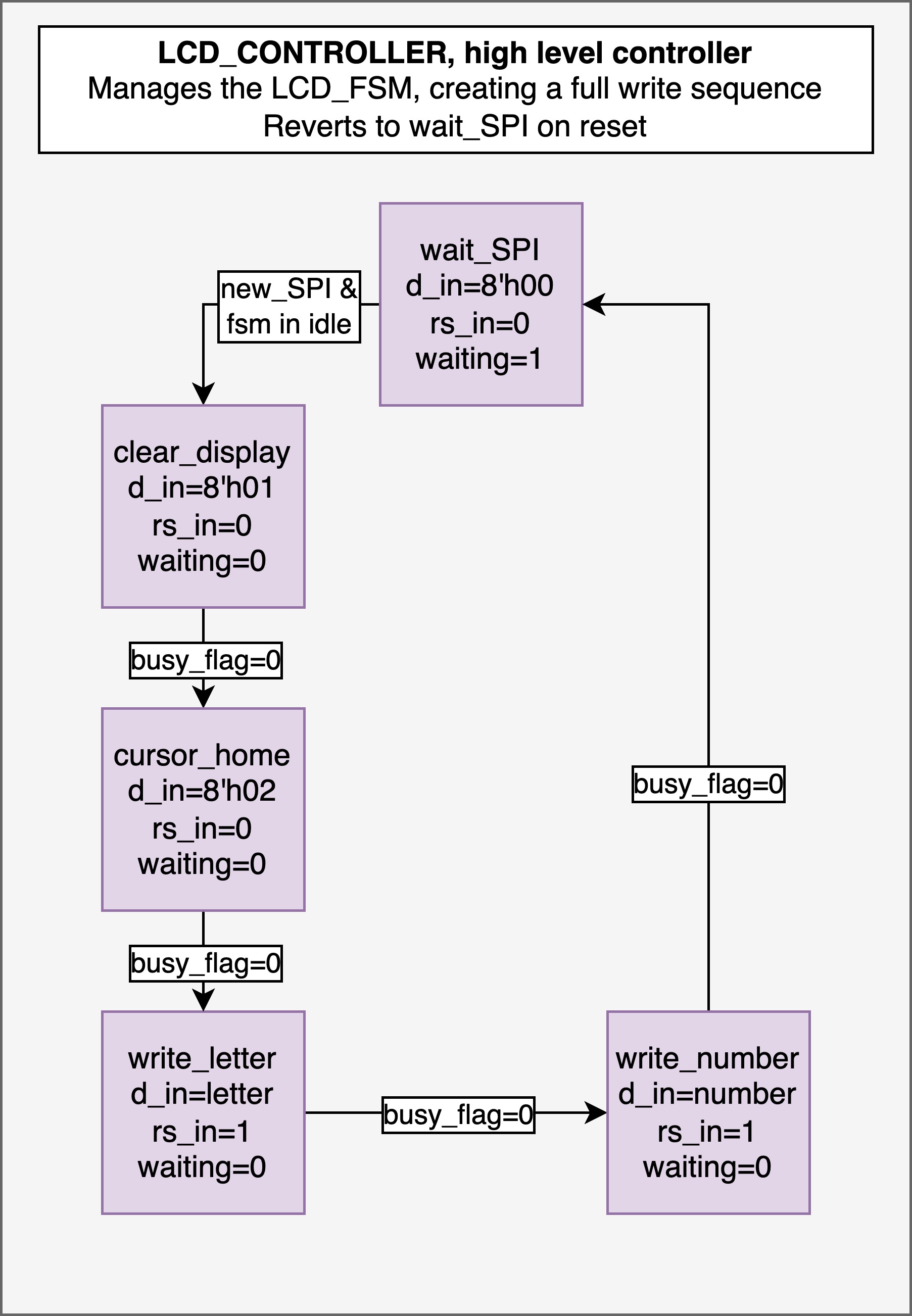
The mid level FSM can be thought of as the director of the low level FSM. This level tells the low level unit what order to send a particular command sequence in. Further, it alone interfaces with the SPI unit, isolating the SPI transactions from the low level LCD architecture. Anything system-specific should happen on this level, allowing the low-level FSM to act like a general-use LCD driver.
The figure below describes the FSM we designed to accomplish this middling function. Note that it idles in the wait_SPI state until the SPI module signals that a new transaction has been received by setting new_SPI.

Converter Module
The converter module is a purely combinational piece of logic which converts, at any given time, the current frequency value stored in the frequency register to a corresponding letter and note. The rest of the timing and system control is handled by the synchronous units in the SPI module and the Controller module.
SPI Module
This module handles the SPI data coming from the MCU. It contains a shift register system which adds the incoming sdi input data to a raw_frequency register, and which sends a new batch of data to the true frequency register when a SPI transaction has finished and the Chip Select line goes high. This transaction ending triggers the SPI module to send out the internal signal new_SPI, which communicates with the controller module to trigger a new printing cycle.